Because of the holidays, TI E2E™ design support forum responses will be delayed from Dec. 25 through Jan. 2. Thank you for your patience.

TCA9554: TCA9554 Input Wiring

Part Number: TCA9554
Other Parts Discussed in Thread: PCF8574, , TCA9534

Tool/software:

Hi everyone,

I'd like to use the TCA9554 as a replacement for PCF8574 in an 8-input I2C button interface. The schematic looks as follows:
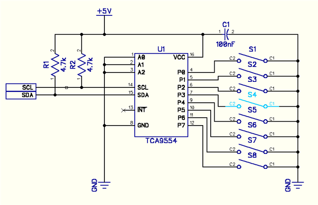
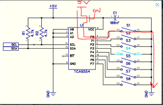
I understood from the datasheet that all ports of the TCA9554 have internal pull-ups, so I omitted them here. Would this configuration work correctly, without any initialization of the inputs needed? In the datasheet example Figure 26 (page 24) the switch at P5 connects to VCC (it is not clear to me why?) and has an additional resistor.

Bonus question: Would you recommend any kind of additional input protection (z-diodes, caps, resistors, ...) if the switches are connected with longer cables (1.5m)?

Best,

sarnold

  • The switch connected to P5 in figure 26 would not work because the input voltage is at VCC in both switch states. You are correct that the input must be switched to GND.

    Initialization is not needed, but the TCA9554 is not software compatible with the PCF8574.

    The TCA9554 and PCF8574 have internal ESD protection, but it is designed only for ESD events that happen during automated assembly. With switches that are touched by humans, additional ESD protection would be a good idea. I'd add clamping diodes to VCC/GND, and a small series resistor between the diodes and the pin to limit the current.

  • Sarnold,

    I understood from the datasheet that all ports of the TCA9554 have internal pull-ups, so I omitted them here. Would this configuration work correctly, without any initialization of the inputs needed? In the datasheet example Figure 26 (page 24) the switch at P5 connects to VCC (it is not clear to me why?) and has an additional resistor.

    I don't think the application schematic on page 24 is correct for P5. Like Clemens said, the switch would not work because the input voltage is at VCC in both switch states. This should be switched to GND. 

    Please see Clemens comments for additional ESD protection circuitry that could be implemented. 

    Regards,

    Tyler

  • Thanks, that is very helpful to see the issue is indeed in the datasheet. I will add additional ESD protection as you suggested. Do you think there would be any advantage in my case to switch to TCA9534 and external pull-ups?

  • It does not matter.

  • Hi Sarnold,

    Switching to TCA9534 gives you the advantage of selecting PU resistance values. If you opt for the TCA9554, the PU resistance is fixed at 100k. 

    I also would like to point out in your design that there is potential for high current path. 

    If you were to accidentally configure the TCA9554 as an output and a switch is closed, there is no series limiting resistance in place. You would effectively have the Ron of the PU FET to 5V shorted through a small switch resistance (S1) to GND. This could potentially break the part or the switch in series. 

    I might recommend some extra series resistance on either side of S1 just to be safe. If the RDS_ON of the FET is 0 ohm, 5V / 220 ohm = 22.7 mA. 

    A 220 ohm series resistance before and after the switch might not hurt. This is just a recommendation in case you program the device wrong the first time. 

    Regards,

    Tyler