This thread has been locked.

If you have a related question, please click the "Ask a related question" button in the top right corner. The newly created question will be automatically linked to this question.

TCAN4550-Q1: mux /WKRQ and /INT

Part Number: TCAN4550-Q1

Tool/software:

Hi team,

my customer is using TCAN4550-Q1 in their design and their MCU has limited I/O, therefore they are seeing if it's possible to mux WKRQ and INT to the same I/O port.

They want to configure the MCU pin to wake up source before system go to sleep (to use WKRQ for CAN wakeup) , and during normal operation configure the MCU I/O to abnormal interrupt (nINT). Does you think it is workable?

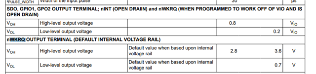
I checked datasheet and found the VI/O threshold is marginal for 3.3V system, do you see any other risk?

Thanks

Scarlett

  • Hi Scarlett,

    This might work but would require some extra register writes to prevent the nWKRQ pin from interfering with the nINT pin during normal operation.

    By default the nWKRQ pin will be driven high to 3.6V when the device is in Sleep Mode.  This internal 3.6V rail is derived from the VSUP which is always on in Sleep Mode unlike the VIO voltage rail which is assumed to be disabled to save power.  Once the device sees a wake-up event it will transition to Standby Mode and the nWKRQ pin will be driven Low until the device is placed back into Sleep Mode.  Therefore, by default the nWKRQ pin will hold the nINT pin low if they are directly connected together in this configuration and there will be no way for nINT to signal an interrupt or generate a "high" through an external pull-up resistor.

    However nWKRQ pin can be configured to be an open-drain just like the nINT pin which will require an external pull-up resistor to VIO.  In this mode the nWKRQ pin can be connected together with nINT because they are both open-drain and either one can pull the line Low to signal an interrupt.  The nWKRQ is a dedicated wake-up interrupt in this configuration and unfortunately there is no advanced notification available when in this mode.  It will only be able to provide the wake-up signal at the same time as nINT because they are both set by the WKRQ bit in the Interrupt register.

    So normally connecting the two together would not be recommended.  But IF the customer is willing to change the nWKRQ pin's configuration between these two modes before entering sleep mode, and then again right after a wake-up event, it might be possible.

    The idea is that prior to entering Sleep Mode, the nWKRQ pin should be set to the default voltage configuration that will drive the pin to the 3.6V while in Sleep Mode.  Then when a wake-up event is detected, it will be driven Low to signal the wake-up event to the MCU.

    After the MCU has processed the wake-up event and re-initialized, it will need to change the nWKRQ pin into the open-drain mode so that the nINT pin can be used normally.  The nWKRQ pin should not cause any other interrupt other than the wake-up event which has already occurred, so this just prevents the nWRQ pin from interfering with nINT during normal operation.

    But, it should be noted that doing this could cause some back-feeding of the VIO rail from the nWRQ pin through the pull-up resistor to VIO because nWKRQ will be driven to 3.6V and VIO is assumed to be disabled (i.e. Low).  So the customer would need to consider this and determine the risk or any counter-measures they need to take depending on the devices connected to VIO in their application.

    Regards,

    Jonathan