Tool/software:
Hello, when using onet1101L, I found that the output pulse width is much wider than the input pulse width, and the width of the output pulse width is more than twice the width of the input pulse width; The input frequency has been tested between 1GHz and 5GHz, and the results are the same; Taking the following waveform as an example:
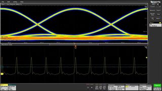
Input waveform
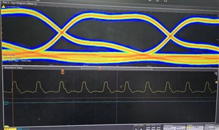
Output waveform DOUT+
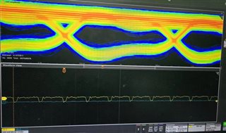
Output waveform DOUT-
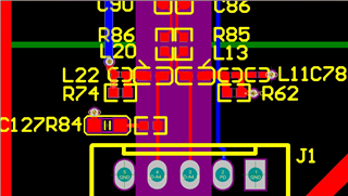
The load is a laser diode,The PCB output has a 50 ohm impedance, and the impedance design is based on the<slla311>released by TI。
May I ask how to solve this problem? Looking forward to your reply!