This thread has been locked.

If you have a related question, please click the "Ask a related question" button in the top right corner. The newly created question will be automatically linked to this question.

SN65LVDT33: Unexpected +- 1000ps jitter in data signals due to interference on multiple LVDS lines

Part Number: SN65LVDT33

Tool/software:

Hello,

We're seeing an unexpected issue with the SN65LVDT33 part we are using on a board, where we are seeing higher-then-expected jitter on an output signal of the chip when sending a e.g. a 75Mhz clock through it (LVDS->SE):

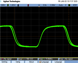
  == SE output, containing +- 1ns jitter. (2 signals driven on chip)

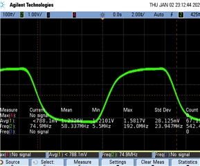
   == LVDS input - very low jitter (2 signals driven on chip)

(We don't see this jitter on the LVDS coming in to the chip)

Interestingly enough, the jitter goes "away" if only one of the 4 channels of the chip is driven with this 75Mhz signal.  


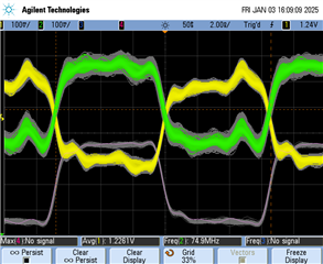
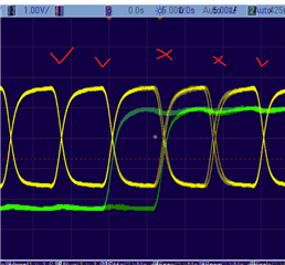
The scenario are now using to easily demonstrate this behavior, is to send a 10Mhz clock on one LVDS pair, and a 75Mhz clock on the second (yellow).
After taking some more scope images, it becomes clear that the "glitching" on the 75Mhz line occurs specifically when the other 10Mhz line (green) is going through a rising edge transition.
The below image was capture triggering on the rising edge of the slow signal, and is overlayed onto itself and shifted in paint. You can see how initially the 75Mhz periods are very clean, and at the moment when the rising edge of the slow/green "couples in", the rising edge of the 75Mhz signal is slightly delayed, causing the jitter effect (which is also seen above in the more simple scope image, "overlayed" by the scope itself, but not showing the exact correlation with the other signal).

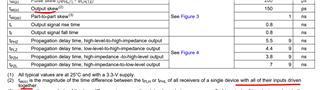
The datasheet lists the following limits

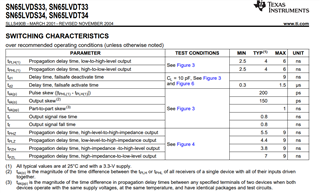
Practically, we had expected some jitter around the order of 150ps - not the 1000 ps we are seeing now.

Is this a known limitation?This behavior is somewhat suprising to us.

Thanks in advance for your feedback!

Kind regards,

Arnout

  • Hi Arnout,

    Thank you for your question.

    The expected jitter is comprised of several factors, such as the data rate and cable length. Please refer to this document that tests the jitter on the SN65LVT33EVM: How Far, How Fast Can You Operate LVDS Drivers and Receivers?

    Depending on your test setup, you may be operating on the edge of the max date rate at 75MHz. You could try this test again by ensuring the test parameters and frequencies are in line with the recommendations from the document.

    Thanks, Amy

  • Hello Amy,

    Allow me to clarify: We are not sending this LVDS signal over any cable. The signal travels from an FPGA over board-to-board connectors to the transceiver, which is less than 10cm away. The jitter should not be this high.

    This is a long shot, but I wanted to check something that could possibly explain this:

    The datasheet mentions some output skew. It's not like the receiver actually tries to -align- incoming transitions, or does it? (in order to "clean up" the signal, and provide better signal-to-signal skew). 
    If it were, it would explain what I am seeing. Such "aligning" would, by definition, slightly delay one signal based on what the other does, which in my case would explain what I am seeing (sometimes delays upon coincidental transitions, otherwise no delay).
    But .. again, I would be somewhat surprised if the chip was actually designed this way. But perhaps you could clarify that?

    Thanks for your feedback!

  • Hi Arnout,

    Thanks for clarifying and providing this information. The device does not try to align the outputs - rather, the output skew metric is related to the unintentional mis-alignment of multichannel outputs. 

    Could you provide a schematic to review?

    Thanks, Amy