This thread has been locked.

If you have a related question, please click the "Ask a related question" button in the top right corner. The newly created question will be automatically linked to this question.

SN65DP159: Schematic Review Request for SN65DP159

Part Number: SN65DP159

Tool/software:

Dear TI Support Team,

I am currently working on a design using the SN65DP159RSB and would like to request your assistance in reviewing our schematic to ensure it is correctly implemented.

Specifically, I would like confirmation on:

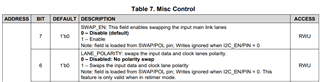
  1. Whether the differential signal P/N swap in our design requires any modifications.
  2. If there are any other potential issues or recommendations for the circuit.

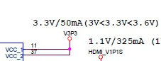
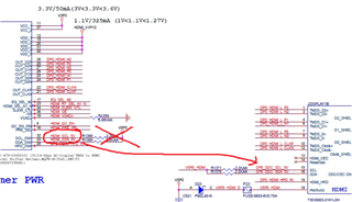
I have attached the schematic for your reference. Please let me know if additional details are required.

By the way, if there is a way to adjust the signal strength for this IC, I would appreciate your advice.

Thank you for your assistance!

  • Hi Tom,

    1. I see that you swap the P/N lines before and after the SN65DP159. This will not work because the SN65DP159 does not support polarity swapping on the HDMI interface. You can swap the polarity on the input DP interface by setting register 09h bit 6 in I2C mode.

    2. I recommend adding 0.1uF capacitors to GND near the VCC pins on our device to mitigate noise on the power line

    3. You need to connect the SCL/SDA_SNK lines from the SN65DP159 to the SCL/SDA pins on the HDMI connector. Right now you have these as separate nets.

    Best,

    Shane