- Ask a related questionWhat is a related question?A related question is a question created from another question. When the related question is created, it will be automatically linked to the original question.
Tool/software:
Hi Ryan,
I got the S parameters of TS3DV642-Q1 from you two months ago. I have some questions, would you please help confirm it ASAP? we really need to make the S parameters clear to proceed with our simulation.
We are going to use TS3DV642RUATQ1 for MIPI CDPHY application and CDPHY exist at the same switch.
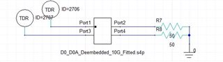
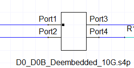
1) could you please clarify each port connection? Below shows your S parameter, but we do not know which port should be connect to D0+、D0-、D0+B、D0-B.
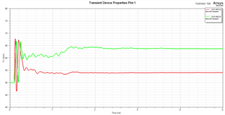
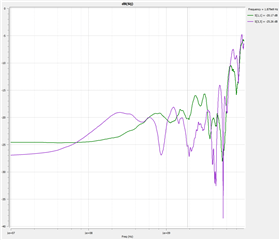
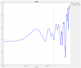
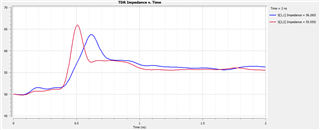
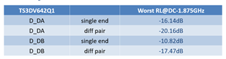
2) Below shows the summary for the S parameters, would you please let me know why the sing end performance is so worse? As for CPHY which is single end, we need the RL meet customer's spec.
3) What's the set up to get the S parameters? Would you please share me with the EVB board deign file and the simulation model? We want to know if our set up is same with yours.