This thread has been locked.

If you have a related question, please click the "Ask a related question" button in the top right corner. The newly created question will be automatically linked to this question.

TS3USB221A: Clarification on TS3USB221ARSER OE Pin Behavior

Part Number: TS3USB221A

Tool/software:

Hi Team,

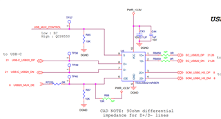
We are using the part TS3USB221ARSER in our design. For your reference, the schematic design is attached.

According to the datasheet, Pin 6 (OE) of the IC is defined as an input, and we have implemented a 10K pull-down resistor to enable the chip's functionality.

However, upon powering up the device, we observed that the OE pin behaves like an output and supplies approximately 2.75V, which contradicts the datasheet specifications.

Could you please provide any insights or explanations regarding this behavior? Let us know if additional details or measurements are needed.

Looking forward to your response.


  • Hi Manikandan,

    There shouldn't be any voltage coming from the OE pin, that is very odd. In the schematic, I see what looks like a control GPIO connecting to the OE pin. Is this actively sending any signal to the OE pin?

    Are the D+/D- being used for normal USB2 activity?

    Would it be possible to test different units, or maybe an EVM, and see if it is still present there?

    Thanks,

    Ryan