This thread has been locked.

If you have a related question, please click the "Ask a related question" button in the top right corner. The newly created question will be automatically linked to this question.

LMH1228: LMH1228

Part Number: LMH1228
Other Parts Discussed in Thread: LMH1297EVM, LMH1297

Tool/software:

Hello everyone!

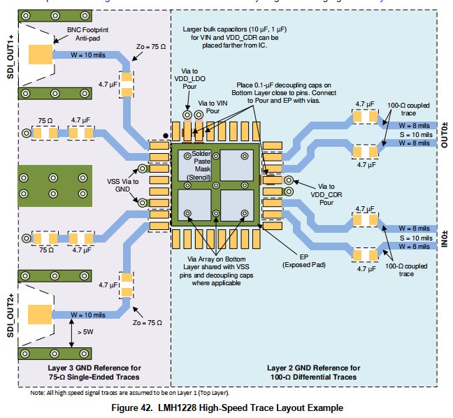
I'm develop a project using LMH1228 and I noted that in the page 36, Layout Example on datasheet, is drawing the isolated area for BNC connector with green areas arround.

Generaly the BNC connctor has external enclousure grounding in the PCB with the ground plane, but in draw that I mentioned above I'm doubit where the BNC ground is conected?

Somebory can help me please?

Thanks

  • Hi Marcelo,

    Hope you are doing well, The BNC connector will connect directly to the ground plane from the top layer of the PCB. The three vias are going to be the connection point to the reference ground for the 75 ohm signal, at layer 3.

    Make sure to maintain a 5W or greater distance between the signal trace and any ground vias for the BNC connector.

    Best Regards,

    Nick

  • Hi Nick,

    I'm fine thanks, and you?

    Thanks for answering me.

    I drew the board layout as shown in the datasheet, that is, in the part intended for the output BNC connectors I only left layer 3 exposed with the separation between the GNDs because that is how the drawing shows it.

    I understood from your answer that the GND plane of the other layers must also be present in the SDI signal output section, is that right?

    What would this BNC footprint Anti-pad identification be that is shown in the datasheet? I understand that it is a region closest to the positive terminal of the BNC connector that must be isolated without receiving any "signals" from the GND planes of the board; is my interpretation correct?

    Regarding the distance, thickness and impedance measurements of the signal tracks, everything is being done very carefully.

    Thanks

  • Hi Marcelo,

    I'm doing well. 

    I understood from your answer that the GND plane of the other layers must also be present in the SDI signal output section, is that right?

    I am confused by this. What do you mean?

    What would this BNC footprint Anti-pad identification be that is shown in the datasheet? I understand that it is a region closest to the positive terminal of the BNC connector that must be isolated without receiving any "signals" from the GND planes of the board; is my interpretation correct?

    Are you asking if the vias should have antipads? If so, then yes.

    Best Regards,

    Nick

  • Hi Nick,

    I designed the PCB with 4 layers.

    As you can see in the image above, there is a division between the right side of the PCB and the left side, where on the right side we have the IN0 input and the OUT0 output. On the left side of the PCB, which is more "directed" towards the output section, we have SDI_OUT1 and SDI_OUT2.

    A dashed line separation of the layers for 100 Ohm differential pairs (right side) and for 75 Ohm differential pairs (left side).

    One of my questions is precisely about this because the understanding I have looking at this drawing is that the GND plane for the 75 Ohm differential pairs should not be part of the GND plane(s) of the rest of the board. Is that right?

    Another question is regarding the dashed area that is in white exactly where it says SDI_OUT1 and SDI_OUT2, which in the drawing is indicated as BNC Footprint Anti-pad. Should there not be any GND plane in this region?

    Thanks

  • Hi Marcelo,

    Thank you for clarifying!

    To answer your first question, I have a clarification and an answer. The 75 ohm traces out of the LMH1228 are single ended, not differential. Ok, and my answer is yes, the 75 ohm GND reference layer will be a layer below the 50 ohm GND reference layer. The reason for this is because the increase in dielectric thickness from the extra layer will increase the reference impedance. The objective is to have a trace impedance of 75 ohms.

    The BNC antipad region should be a complete void through all layers and planes.

    Best Regards,

    Nick

  • Hi Nick,

    Forgive me for insisting, but something is still not clear to me.

    The image I attached in the previous message shows and suggests that on the output side of the board, SDI_OUT1 and SDI_OUT2, there should only be the third layer and the others should not exist in this region of the board; is my interpretation correct?

    Remembering that the output signal tracks are obviously necessary...

    But is the interpretation that only the third layer should exist in this region correct?

    Regards

    Marcelo

  • Hi Marcelo,

    I understand. Here are some photos illustrating what the design is on our LMH1297EVM.

    VDD1 is the 75 ohm reference and GND 1 is the 100 ohm reference.

      GND1

      VDD1

    This is from the LMH1297EVM.brd file that I can send to you by direct message if you would like.

    Best regards,

    Nick

  • Hi Nick,

    Yes, please, send me the LMH1297EVM file by direct message.

    Thank you.

  • Hi Marcelo,

    Nick is currently out of the office.

    This board file can also be obtained through a request to the LMH1297 secure resources folder, available on the LMH1297 product page under the Request more information section.

    Best,
    David

  • Hi David

    Ok, thanks for your information. I downloaded the image that Nick send me.

    Do you view the image that I send to Nick?

  • Hi Marcelo,

    Today (Feb 17) is a holiday in the US. Nick will get back to you tomorrow regarding your question.

    The request link I’ve suggested would allow you to access the EVM’s BRD file.

    Best,

    David