This thread has been locked.

If you have a related question, please click the "Ask a related question" button in the top right corner. The newly created question will be automatically linked to this question.

TLIN2029-Q1: the wake up signal from LIN bus

Part Number: TLIN2029-Q1
Other Parts Discussed in Thread: TLIN1021A-Q1, TLIN2021A-Q1, TLIN2029A-Q1

Tool/software:

Dear team,

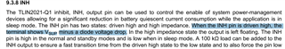
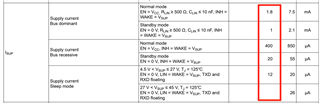
our customer want to know if they are using TLIN2029-Q1 with the following configuration:

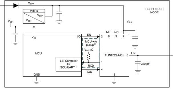
under LIN2029-Q1's sleep mode, MCU is also in sleep mode (I/O PIN, Vdd are both pulled to low)

at this circumstance, if TLIN2029 receives a LINBus wake-up signal, how to wake up MCU as well.

Best regards,

Hank Lin

  • Hi Hank,

    This is done when the TLIN device detects LIN wake-up signals when connected to a GPIO pin on the MCU. This effectively wakes up the MCU when the LIN bus receives a wake-up signal. You may also see TLIN1021A-Q1 with additional wake-up capabilities, thanks.

    Best Regards,

    Michael.

  • Dear Michael,

    may I double check...

    do you mean we can achieve the wake-up on TLIN2029-Q1 by tying LINBUS to MCU's one GPIO for triggering?

    or we can only achieve this wake-up capability by using TLIN1021A-Q1?

    Best regards,

    Hank Lin

  • Hi Hank,

    I meant TLIN2029-Q1 documents 2 methods for waking-up highlighted in section 7.4.4 of the data sheet while TLIN1021A-Q1 documents 3 methods as highlighted in 9.4.4 of the data sheet. Hence giving customers more flexibility for which ever option works best, thanks.

    Best Regards,

    Michael.

  • Dear Michael,


    I want to check whether my understanding is correct for Delta's following questions:

    Q1. (on TLIN2021A-Q1)

    according datasheet, V_INH voltage level almost equal to V_sup.

    According to the datasheet statement, may I ask further about the typical voltage drop rating of the diode?


    Q2. (The question for both TLIN2029A-Q1 and TLIN2021A-Q1)

    According to the datasheet, the logic output/ input (TXD/RXD)'s operation range is from 0V to 5.25V.

    Delta wants to know whether a 3.3V logic level could be effectively high


    Q3. (The question for both TLIN2029A-Q1 and TLIN2021A-Q1)

    the power consumption of the TLIN devices, taking TLIN2021A-Q1 as the example...

    Delta wants to supply the TLIN devices with a 12V voltage rail. Can I just easily multiply the typical current rating to the 12V to estimate the power consumption? 

    and what is the reason that the maximum of the currents that can be twice of typical value?  these are wide range.

    Best regards,

    Hank Lin

  • Hi Hank,

    According to the datasheet statement, may I ask further about the typical voltage drop rating of the diode?

    The voltage drop is typically around 0.7 V.

    Delta wants to know whether a 3.3V logic level could be effectively high

    Yes, 3.3 V is higher than the VIH threshold so no concerns for TXD input. RXD output is open drain and can be pulled to 3.3 V with out concerns.

    Delta wants to supply the TLIN devices with a 12V voltage rail. Can I just easily multiply the typical current rating to the 12V to estimate the power consumption? 

    and what is the reason that the maximum of the currents that can be twice of typical value?

    Please help see How can the power consumption of a CAN transceiver in active operation be calculated?. Also note the range accounts for worse case  PVT variations for different conditions while typical accounts for standard conditions. Hence, it is common to specify such ranges, thanks.

    Best Regards,

    Michael.