Part Number: TUSB4041I
Tool/software:
Hi,
I have some doubts concerning TUSB4041I power-up sequence.
It is described in "TUSB4041I Four-Port USB 2.0 Hub" Manual (SLLSEK3E –JULY 2015–REVISED SEPTEMBER 2017 ), page 10

I followed the reference design - EVB: https://www.ti.com/lit/ug/sllu227a/sllu227a.pdf?ts=1739296190986&ref_url=https%253A%252F%252Fwww.google.com%252F
where chain of power regulators is used:
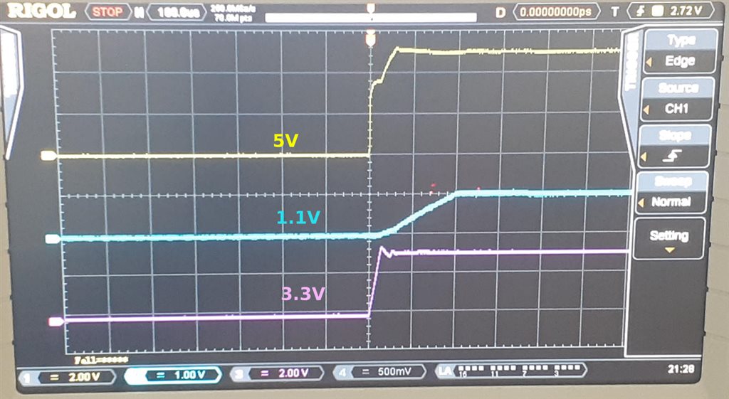
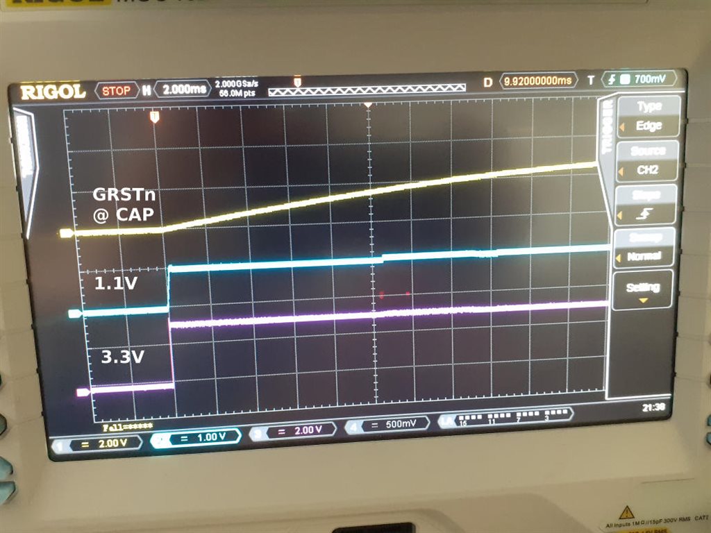
5V -> 3v3 -> 1v1
As it was there I also connected GRSTn to GND with 1uF capacitor.
I see some incosistency in that cited documentation and solution in the EVB:
- chain of power supply regulation in the EVB does not assure that 1v1 supply comes before 3v3 (1v1 power is regulated from 3v3),
- above is inconsistent with requirement in the note [2] in chip manual,
- input GRSTz is pulled up to 3v3 rail if I properly read documentation, isn't it?
- documentation states that low level on GRSTz (i.e. asserted GRST) forces the chip to be non-fuctional ("When the GRSTz pin is asserted, the device is completely nonfunctional.")
(i) I worry that circuit in the EVB does not provide proper sequence of power-up,
(ii) Why is the requirement [2] in chip manual if GRSTz is kept low from power-on by capacitor to ground on the pin?
(iii) Is the requrement [2] in chip manual correct? It looks for me like it is opposite condition.
Kind regards,
Piotr Romaniuk