This thread has been locked.

If you have a related question, please click the "Ask a related question" button in the top right corner. The newly created question will be automatically linked to this question.

DP83867E: Regarding the layout design of the DP83867E.

Part Number: DP83867E

Tool/software:

Hi team,

In the datasheet’s section 8.2.2.2.1 MDI Layout Guidelines, it states, “MDI traces must be 50Ω to ground and 100Ω-differential controlled impedance.”

My customer is facing an issue where trying to meet both the 100Ω differential and 50Ω single-ended requirements results in a layout where the differential signal traces are spaced further apart compared to a layout with only 100Ω differential traces.

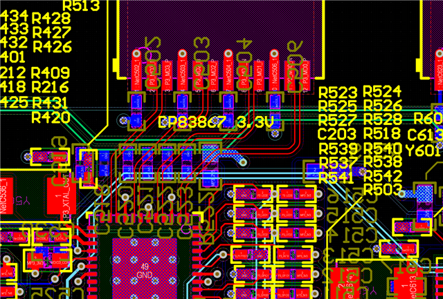
I would like to show the layout diagram of the DP83867E SGMII EVM as an example of a layout pattern. Could you provide this diagram?

Also, is there a priority among the three requirements: 100Ω differential, 50Ω single-ended, and the spacing between differential signal traces?

What is the acceptable design tolerance for the 100Ω differential and 50Ω single-ended impedance?

Best regards,

  • Hi,

    The tolerance on the MDI is 100ohm differential +/- 10%.

    The 100ohm differential is between TD_P_A and  TD_M_A,  TD_P_B and TD_M_B, TD_P_C and TD_M_C, TD_P_D and TD_M_D. The trace width and spacing, plus the dielectric thickness need to be calculated to achieve the desired differential impedance. You can see in the below picture how the differential signal is being routed between the DP83867 and the external transformer.

    Would you please accept my friendship request so I can send you the actual EVM file as a reference?

    Thanks

    David

  • Hi David,

    Thank you for your reply.

    Is it correct to understand that as long as the differential 100Ω part falls within ±10%, communication will be established?

    I couldn’t confirm the friend request, so I have sent a request.

    I would appreciate it if you could provide the EVM file.

    Also, may I show the layout diagram part of the provided file to the customer?

    Best regards,

    Kyohei

  • Kyohei-san

    I sent the board file to you in a private message, would you please check?

    You can also share the layout diagram part of the provided file with your customer.

    Thanks

    David

  • Hi David,

    I checked the file, thank you.

    Additionally, while the differential impedance is around 100Ω with a tolerance of ±10%, is it correct to understand that communication will still be established even if the single-ended impedance deviates to around 55-60Ω (±10-20%)?

    Also, while the differential impedance tolerance of 100Ω is ±10%, does this refer to design tolerance? When the board is actually manufactured, there may be additional errors due to manufacturing tolerances. Is there data available that includes the acceptable tolerance values considering manufacturing errors as well?

    Best regards,

    Kyohei

  • Kyohei-san

    The 100ohm differential +/-10% includes the manufacturing tolerances. The +/-10% is the standard industry tolerance and most PCB Fab can support it. The single end impedance should be 50ohm +/- 10%.

    If there is an impedance mismatch, then the impedance mismatch will decrease throughput, sometimes significant enough to cause communication failure. The mismatches cause signal reflections that prevent maximum power from being transferred beyond the point of reflection.

    Thanks

    David