This thread has been locked.

If you have a related question, please click the "Ask a related question" button in the top right corner. The newly created question will be automatically linked to this question.

SN65DSI84: disable Hsync and Vsync

Part Number: SN65DSI84

Tool/software:

Hi,

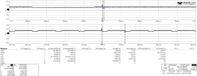
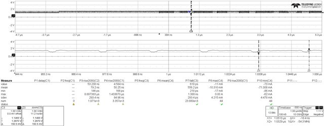
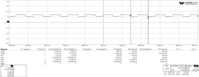
we have a product that uses sn65dsi84 as a bridge from a Linux CPU module that outputs MIPI-DSI to a dual-channel LVDS panel.

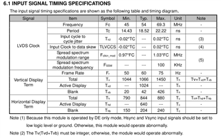
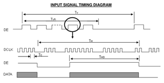
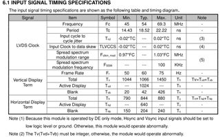
The panel datasheet states the following:

"Because this module is operated by DE only mode, Hsync and Vsync input signals should be set to low logic level or ground. Otherwise, this module would operate abnormally"

Indeed, in order to make the panel to display our boot logo we had to modify the Linux driver and hard-code Hysnc/Vsync pulse width registers to 0. In this way, we can "simulate" the fact that they must not be used; without this little trick, the screen would simply go blank.

I would like to understand if our "solution" is the intended one for such situations, or if there is a better/correct way to achieve this? I'm asking in particular because we see bit 0xE5.7 being set to 1, which as far as I understand can be ignored in our case as we don't rely on HS/VS.

Thank you in advance!

  • Hi,

    Are you seeing an actual issue with your current implementation?

    The first line of a video frame needs to start with a VSS packet, and all other lines start with VSE or HSS. The DSI84 needs to see these packets to generate the HS and VS (horizontal and vertical sync) signals on the LVDS interface after the delay programmed into CHA_SYNC_DELAY_LOW/HIGH (CSR 0x28.7:0 and 0x29.3:0) and/or CHB_SYNC_DELAY_LOW/HIGH (CSR 0x2A.7:0 and 0x2B.3:0). When configured for dual DSI channels, the SN65DSI84 uses the VSS, VSE, and HSS packets from channel A to generate the HS and VS (horizontal and vertical sync) signals on the LVDS interface, and the VSS, VSE, and HSS packets from channel B are ignored.

    Have you used the DSI Tuner to generate the DSI84 register programming value based on the video panel spec?

    Thanks

    David

  • Thanks for the reply.

    As mentioned, I can correctly see the boot logo (programmed through drivers/video/logo/), and for example I can output noise via `cat /dev/random > /dev/fb` (and I see it changing on repeated commands). Prior to this, I was also able to correctly see the test pattern.

    Here's the relevant datasheet snippet from the panel, at the bottom the quote from my main post:

    And here is the timing diagram:


    As you can see, the panel makes no use of sync packets.

    Indeed, prior to setting CHA_HSYNC_PULSE_WIDTH_LOW/HIGH (CSR 0x2C.7:0 and 0x2D.1:0) and CHA_VSYNC_PULSE_WIDTH_LOW/HIGH (CSR 0x30.7:0 and 0x31.1:0) to zero, the panel output was simply blank, and the panel would go into stand-by shortly after.

    I did use DSI Tuner at some point at the beginning when playing directly with sn65dsi84 via i2c. However, when switching to Linux I must admit I ported what I could in the device-tree, and started debugging the values calculated / hard-coded in the kernel driver. Afterward, I patched the driver and fine-tuned the wrong values based on the various datasheets (sn65dsi84, panel, ...) I had available. I then recently turned those hard-coded fixes into some more appropriate device-tree properties, however this is all still downstream at the moment.

    Thanks

    Alessandro

  • Alessandro

    Can you measure the line time on the DSI input and the LVDS output with Hysnc/Vsync pulse width registers set to 0? It is important to make sure the line time (time from HSYNC to HSYNC) on the DSI input matches the line time on the LVDS output. The line time on the LVDS output is the total amount of horizontal pixels divided by the LVDS clock frequency. You can measure the line time on the DSI input with an oscilloscope by zooming in on the data stream on of the data lanes like below:

    Thanks

    David

  • I have captured the signal with an oscilloscope, but unfortunately it looks way different from yours. Therefore, I'm not sure what to measure exactly or how. At the bottom of this message I've attached some screenshots of some random DSI/LVDS lanes + LVDS clock.

    Also, as reference, the  LVDS output clock frequency is ~54 MHz and the total horizontal pixels are 844. Both values can be also read from the datasheet snippet I attached to my previous post.

    DSI0 (1):

    DSI0 (2):

    DSI3 (1):

    DSI3 (2):

    LVDS2:

    LVDS clock:

    Thank you

  • Alessandro

    Can you clarify that the LVDS panel info provided below is for one half of the display or the entire display?

    If I assume the timing is for one half of the display, then the line time at the DSI input is Htotal / Pixel clock = 844/54 = 15.63us, which matches your DSI input measurement. Are you able to see the image being displayed in this case?

    I am also assuming the DSI CLK is 324MHz, and you are using divider of 6 to generate the 54MHz LVDS clock.

    Thanks

    David

  • Yes, your assumptions are correct: the datasheet info is for a single LVDS channel, therefore I have the horizontal attributes doubled in my device tree; also, the DSI clock is indeed 324 MHz and the divider is set to 6.

    As I mentioned in my previous posts, I can see the image correctly on my panel if I set the H/Vsync pulse width to 0. However, this is a "hack" I'm not happy about, and I'd like to understand better why does this work and if this will create issues in the future.

    My main concern is that the panel expects that the H/Vsync signals are low voltage/grounded, but there is no way to do this on sn65dsi84 except to force the pulse width to zero. This works, meaning that the panel can correctly show our boot logo or random noise, but it is an ugly workaround which is probably masking an incompatibility between the panel and the sn65dsi84. As a symptom, I can see bit 0xE5.7 constantly set to 1.

    This is the whole point of my question. Given that hard-coding the H/Vsync signals pulse width to zero in sn65dsi84 makes the panel correctly display out boot logo, can I expect the whole signal chain to work reliably, even though the panel requires low voltage H/Vsync signals? What about 0xE5.7 error bit in this scenario?

    Thanks!

  • Hi,

    There is no need to match horizontal or vertical video CSR configurations to the DSI input values except for the CH*_ACTIVE_LINE_LENGTH (number of active pixel). In other words, as long as the line time is met, the blanking parameters on the LVDS side do not need to exactly match the blanking parameters on the DSI side. However, the active pixels always need to match. And we did verify that the line time is matching correctly. 

    For the register 0xE5, bit 7 will get set because the line time measurements coming from the DSI source does not line up with that the register are set to. We will have to ignore it since the line time from the DSI source does match with the line time of the LVDS panel.

    Thanks

    David

  • Thanks for the explanation and the support David!