This thread has been locked.

If you have a related question, please click the "Ask a related question" button in the top right corner. The newly created question will be automatically linked to this question.

PCF8575: managing I/O with current protection Chip

Part Number: PCF8575
Other Parts Discussed in Thread: TCAL6416, TCA6416A,

Tool/software:

Hi All,

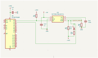
I have the schematic below to validate. 

  1. P0 as output , P1 as input.
  2. At power up I need P0  is not to "0" (ground) otherwise it will be shutoff my current protection chip which i want to avoid. From what i see at startup all GPIO are high so I will be safe , right?
  3. After power up I need to configure P0 as output but to not going to zero. How can I do that ? Can I:
    1. write the ouput register relative to "P0" to high 
    2. configure P0 like an output ?

Please an help will be appreciated to finish the design.

Thanks a lot

  • The I/O pins of the PCF are inputs and outputs at the same time. They drive strongly low or weakly high; when high, external devices can override the voltage by driving the pin low.

    At power up, all pins are high; this already is what you want.

  • Hi Clemens, thanks for reply.

    Cant understand what means "They drive strongly low or weakly high; when high, external devices can override the voltage by driving the pin low"

    Can you confirm that after configuring P0 as output the value on that pin is not groundend (0V) unitl I push it to "zero"  with the right I2C command?

  • Pins cannot be configured as output or input. To use a pin as input, configure it to output high (which is the default).

    The default state of all pins is high.

  • Hi Clemens, 

    thanks again.

    Of course I'm not going to use a Pin as input or output at the same time during  the normal operating phase . Every pin will be configured or just like an input or just like an output and just like in the Datasheet diagram below (hybrid configuration)

    In addition I need to know the following:

    • after power UP the MCU/MP master  will configure the P0 like an output pin.
    • what happens to this pin after configured as output ? will it preserve the high voltage like before to be configured as an output (default high)  ? or will it be open drain (float) ? or anything else?

    I need to avoid the pin goes to ground (0V) after configured as an output because if so I have to pull it high again with an I2C transition (MCU will send a command to push the output pin to 3,3V) in order to avoid shutting down the downstream chip.

    Hope you can support,

    Thanks.

  • Hi Nicola,

    • after power UP the MCU/MP master  will configure the P0 like an output pin.
    • what happens to this pin after configured as output ? will it preserve the high voltage like before to be configured as an output (default high)  ? or will it be open drain (float) ? or anything else?

    If P0 is written HIGH, then the P0 is pulled up weakly acting as an output HIGH, but can be easily overwritten by an external output (meaning that the pin is an output high, but also acts as an input if it were to be driven externally LOW). 

    This is what we mean by quasi-bidirectional input/output pins. 

    If you need strict outputs that pull HIGH regardless of an external output to the pin, then consider any "TCA" or "TCAL" IO expander. 

    TCA6416A / TCAL6416 for example. 

    Regards,

    Tyler

  • Hi Tyler, thanks for supporting me.

    If you look at my circuit above , P0 will be connected to the input PIN  of an external chip (pulled up by a resistor). There will be no other external circuit trying to putting the P0 pin  to LOW  while is HIGH or putting it to HIGH  when is LOW.  My schematic is similar the one if I had to drive the "EN" pin of an external  LDO. Have you such example to share ? Have you used the Px pin to on/off external open drain enable/disable PIN (example  LDO, switch) ?

    Hope you can help since I dont want to change the schematic with PN  TCA64xx series for now.

    Nicola

  • Your schematic will work.

  • Hi Nicola,

    The way you are using the PCF8575 will work. I don't see a need for a schematic change. 

    Regards,

    Tyler