This thread has been locked.

If you have a related question, please click the "Ask a related question" button in the top right corner. The newly created question will be automatically linked to this question.

DS250DF410: DS250DF410/LMK04832

Part Number: DS250DF410
Other Parts Discussed in Thread: LMK04832,

Tool/software:

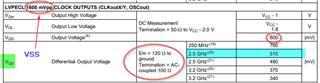
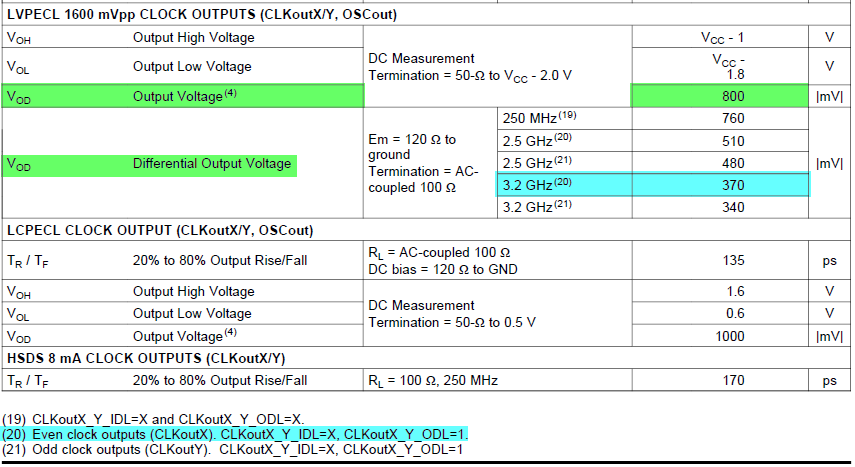
I am interested in using the DS250DF410 for PRBS testing at 25.78125GHz in a 3U VPX Backplane. My plan is to design a 3U VPX Plug-In Card that will contain a DS250DF410 Re-Timer. Four of the Tx Ports {x4} and Four of the Rx Ports {x4} will be routed to the 3U VPX Connector [Data Plane]. In the Backplane, the Data Plane from the 3U VPX Re-Timer Plug-In Card is routed to a 3U VPX Switch Card. When using the DS250DF410 to "Generate" PRBS Data @ 25.78125GHz, I plan to use an LMK04832 [Also located on the DS250DF410 3U VPX Plug-In Card] to generate (4) Copies of a Sub-Rate Clock of 25.78125GHz/16 = 1.611328125GHz. Each Copy of the 1.611328125GHz Clock from the Output of the LMK04832 will be AC-Coupled to Each of the Rx Ports on the DS250DF410. The (4) Output Clocks from the LMK04832 @ 1.611328125GHz will be configured as LVPECL 1600mVpp. From the Data Sheet of the LMK04832 shown below, the Expected Vod @ 3.2GHz is 370mVpp when Each Output Leg is Terminated to Ground with a 120Ohm Resistor, and then AC-Coupled to a 100Ohm Load.

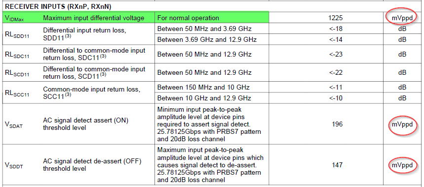
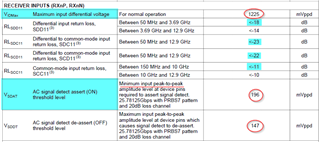
From the Data Sheet of the DS250DF410 shown below, Maximum Vid = 1225mVpp and Vdsat = 196mVpp [With Signal Detect Assert = "On"]

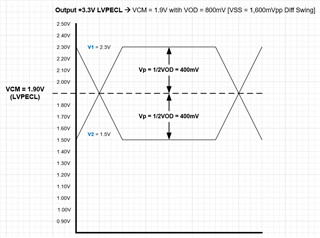
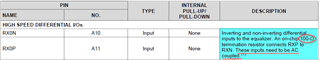
Input Termination to Each DS250DF410 Rx Port is 100Ohms [See Below]:

LMK04832 to DS250DF410 Circuit Shown Below:

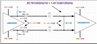
LMK Output is 800mVpp when DC-Coupled and 370mVpp with Each Leg Terminated to 120Ohm and AC-Coupled to a 100Ohm Load [DS250DF410].

Will the Design Concept Described/Shown work properly to Generate PRBS Data @ 25.78125GHz at the (4) Tx Ports of the DS250DF410?

  • Hi Dallas,

    Thanks for sharing details on your design and design considerations.

    In general, using the LMK04832 to generate 1.611328125 GHz clock for DS250DF410 PRBS generation appears to be a sound design.

    • Regarding the LVPECL driver, I'm not as familiar with this driver topology.  Would it be possible to share more details on the selection of Rs?
    • Also, I do have concern regarding the input voltage.  I believe the LMK04832 and DS250DF410 are using different conventions for VOD / VID.  In LMK04832, it's using a definition that VID/VOD = | Vp - Vn |.  Please see section `7.2 Differential Voltage Measurement Terminology` in LMK04832 data sheet.  For DS250DF410, VID/VOD is specified in mVppd.  This is defined as VID/VOD = p-p (Vp - Vn).

      As an example, let's say there is a differential signal where Vp / Vn each swing from 1.5V to 2.3V.  LMK04832 data sheet will say this is VID/VOD = 800 |mV|.  DS250DF410 data sheet will say this is VID/VOD = 1600 mVppd.

      Looking at LVPECL, it's not clear what amplitude a 1.6 GHz signal will have.  I'd speculate that the swing is likely within DS250DF410 VID, but it's not clear how swing varies between 250 MHz and 2.5 GHz.

    • Most high speed Ethernet signals use CML or VML drivers.  I'm wondering if it may be worth considering using the CML output from LMK04832.  The voltage from 250 MHz to 2.5 GHz appears within DS250DF410 VID.

    One additional note is that for the PRBS generator, it's not recommended to enable for than 2 at a time per device.  In your design, I'm wondering if enabling 2 PRBS generators at a time would be sufficient.

    There are two primary reasons for this recommendation:

    • PRBS generator uses a relatively large amount of power and will increase device temperature.  This could be compensated for by adding heat sinking.
    • On similar devices, I have observed that operating the device at the lowest supply corner (2.375V) with multiple PRBS checker blocks enabled can lead to the PRBS checker malfunctioning.  I'm not sure if this behavior extends to the PRBS generator, and this likely pertains to the power network within the device.  If you plan to have 4 PRBS generators enabled, I'd recommend ensuring you can supply at least 2.5V to DS250DF410.

    Thanks,

    Drew

  • Thanks for the Feedback Drew. 

    You are "Absolutely" Correct about Specifying the Outputs from the LMK

    In Section 7.2, there are (2) ways to reference Differential Outputs and Inputs.

    Below is my drawing of Waveform:

    Vp and Vn "Each" Swing between 1.5V and 2.3V. This means Vod = Vp - Vn = 800mV.

    VSS = 2 * Vod = 1600mVpp

    This is "Why" the Output Format on Page 14 refers to 1600mVpp [This VSS = 2 * Vod]

    So, LVPECL 1600mVpp has the Following Output Specification:

    a. Vod = Vp - Vn = 800mV

    b. VSS = 2* Vod = 1600mVpp

    Note: It also says Vod =510mV [VSS = 1020mVpp] @ 2.5GHz, so at 1.611328125GHz, I would expect it to be "Slightly" Higher.

    Now you say that for the DS250DF410, the Inputs are "Specified" as mVppd or VSS with respect to the LMK04832.

    So referencing Apples-To-Apples:

    1. LMK LVPECL 1600 Output
         a. Vod = 540mV @ 2.5GHz

         b. VSS = 1080mVpp @ 2.5GHz

    2. DS250DF410 Input

         a. Vid{max} = VSS {With Respect to LMK} = 1225mVpp

         b. Vid {With Respect to the LMK} = 612.5mV

    So in one sense, if the LMK Outputs 1600mVpp, then it would "Over Drive" the DS250DF41's Input Specified as 1225mVpp Maximum. Do you Agree?

    I have (2) Data Points from the LMK:

    a. 370mV [740mVpp] @ 3.2G

    b. 510mW [1020mVpp] @ 2.5G

    If the Output "Tracks" Linearly with Frequency, then I would expect 687.72mV [1375.47mVpp] @ 1.611328125G.

    This "Still" exceeds the DS250DF410's Maximum input specification of 1225mVpp. Do you Agree?

    Finally, If I "Well" Heat Sink the DS250DF410, with 2.5V "Minimum" Guaranteed Supply at Vcc, then I should be able to run (4) Generators at a time. Correct?

    This will also apply to (4) Checkers as well {I'll need to Well Heat Sink the DS250DF410 and Provide 2.5V "Minimum" Vcc}. Do you Agree?

  • Hi Dallas,

    So in one sense, if the LMK Outputs 1600mVpp, then it would "Over Drive" the DS250DF41's Input Specified as 1225mVpp Maximum. Do you Agree?

    Yes, I agree with this.

    I have (2) Data Points from the LMK:

    a. 370mV [740mVpp] @ 3.2G

    b. 510mW [1020mVpp] @ 2.5G

    If the Output "Tracks" Linearly with Frequency, then I would expect 687.72mV [1375.47mVpp] @ 1.611328125G.

    I also agree with this if output amplitude tracks linearly with frequency.  However, it's not clear to me if this is a good assumption.  You might consider creating a separate thread on this topic so that the clocking group can help advise.

    Finally, If I "Well" Heat Sink the DS250DF410, with 2.5V "Minimum" Guaranteed Supply at Vcc, then I should be able to run (4) Generators at a time. Correct?

    This will also apply to (4) Checkers as well {I'll need to Well Heat Sink the DS250DF410 and Provide 2.5V "Minimum" Vcc}. Do you Agree?

    I agree that taking these steps will likely set you up for success with this design.  However, please keep in mind that this is outside of TI's recommendations, so you'll be doing this at your own risk.

    Thanks,

    Drew