This thread has been locked.

If you have a related question, please click the "Ask a related question" button in the top right corner. The newly created question will be automatically linked to this question.

DS90UB941AS-Q1: Dual-DSI Inputs, 1920x1080, Pattern Generator Help

Part Number: DS90UB941AS-Q1
Other Parts Discussed in Thread: ALP

Tool/software:

Hello,

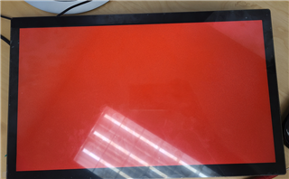
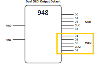
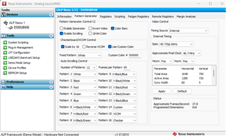
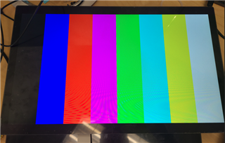
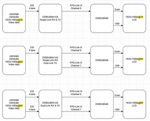
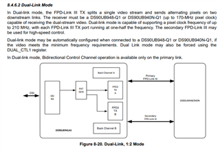
I have the DS90UB941 serializer and a DS90UB948 deserializer.  The LCD I have is 1920x1080, and the pixel clock required is 143MHz.  I need to use the dual DSI inputs due to the pixel clock being higher than 105MHz.  I still need to work out some bugs in my device tree, so I wanted to first test the LCD with the pattern generator.  The 941 datasheet has example code for the Independent 2:2 Mode, but does not include any code for the Dual Mode, so I am unsure what all registers need to be changed.

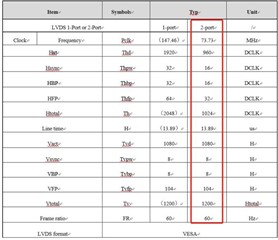
Can you please provide the registers that I need to set for the pattern generator to work with the panel mentioned above?  The timing details for the panel are as follows:

Pixel Clock: 143.28 MHz  (60Hz)
Horizontal Display Area: 1920
Horizontal Front Porch: 24
Horizontal Back Porch: 70 
HSYNC Total Period Time: 2048

Vertical Display Area: 1080
Vertical Front Porch: 16
Vertical Back Porch: 48
VSYNC Total Period Time: 1166

Thank you!

  • Hi Brent,

    Do you have access to our ALP tool? https://www.ti.com/tool/ALP?keyMatch=analog%20launchpad&tisearch=universal_search 

    You can use the PATGEN tab there to generate a script for your specific use case. 

    Please see the attached reference script, "94x PATGEN". Variables can be populated by using the "Pattern Generator" and "PATGEN Registers" tabs in combination in ALP. First, input desired timings and settings into the "Pattern Generator" tab, then press apply. Then, navigate to the "PATGEN Registers" tab and save the registers using the "Save" button. From this output file, variables can then be entered into the "PATGEN Configurations" section of the attached "94x PATGEN" script accordingly.

    Note that registers 0x64 and 0x65 may need to be adjusted if you are using a different operating mode (i.e. internal timing with external CLK, etc.)

    import time 
    devAddr = 0x18
    desAlias0 = 0x58
    PGIA = 0x66
    PGID = 0x67
    
    ## *********************************************
    ## PATGEN configurations
    ## *********************************************
    PGRS =      0x00
    PGGS =      0x00
    PGBS =      0x00
    PGCDC1 =    0x00
    PGTFS1 =    0x00
    PGTFS2 =    0x00
    PGTFS3 =    0x00
    PGAFS1 =    0x00
    PGAFS2 =    0x00
    PGAFS3 =    0x00
    PGHSW =     0x00
    PGVSW =     0x00
    PGHBP =     0x00
    PGVBP =     0x00
    PBSC =      0x00
    PGFT =      0x00
    PGTSC =     0x00
    PGTS01 =    0x00
    PGTS02 =    0x00
    PGTS03 =    0x00
    PGTS04 =    0x00
    PGTS05 =    0x00
    PGTS06 =    0x00
    PGTS07 =    0x00
    PGTS08 =    0x00
    PGBE =      0x00
    PGCDC2 =    0x00
    
    board.WriteI2C(devAddr, PGIA, 0x00)
    board.WriteI2C(devAddr, PGID, PGRS) #PGRS
    board.WriteI2C(devAddr, PGIA, 0x01)
    board.WriteI2C(devAddr, PGID, PGGS) #PGGS
    board.WriteI2C(devAddr, PGIA, 0x02)
    board.WriteI2C(devAddr, PGID, PGBS) #PGBS
    board.WriteI2C(devAddr, PGIA, 0x03)
    board.WriteI2C(devAddr, PGID, PGCDC1) #PGCDC1
    board.WriteI2C(devAddr, PGIA, 0x04)
    board.WriteI2C(devAddr, PGID, PGTFS1) #PGTFS1
    board.WriteI2C(devAddr, PGIA, 0x05)
    board.WriteI2C(devAddr, PGID, PGTFS2) #PGTFS2
    board.WriteI2C(devAddr, PGIA, 0x06)
    board.WriteI2C(devAddr, PGID, PGTFS3) #PGTFS3
    board.WriteI2C(devAddr, PGIA, 0x07)
    board.WriteI2C(devAddr, PGID, PGAFS1) #PGAFS1
    board.WriteI2C(devAddr, PGIA, 0x08)
    board.WriteI2C(devAddr, PGID, PGAFS2) #PGAFS2
    board.WriteI2C(devAddr, PGIA, 0x09)
    board.WriteI2C(devAddr, PGID, PGAFS3) #PGAFS3
    board.WriteI2C(devAddr, PGIA, 0x0a)
    board.WriteI2C(devAddr, PGID, PGHSW) #PGHSW
    board.WriteI2C(devAddr, PGIA, 0x0b)
    board.WriteI2C(devAddr, PGID, PGVSW) #PGVSW
    board.WriteI2C(devAddr, PGIA, 0x0c)
    board.WriteI2C(devAddr, PGID, PGHBP) #PGHBP
    board.WriteI2C(devAddr, PGIA, 0x0d) 
    board.WriteI2C(devAddr, PGID, PGVBP) #PGVBP
    board.WriteI2C(devAddr, PGIA, 0x0e)
    board.WriteI2C(devAddr, PGID, PBSC) #PBSC, if not working try both positive AND negative polarity
    board.WriteI2C(devAddr, PGIA, 0x0f)
    board.WriteI2C(devAddr, PGID, PGFT) #PGFT
    board.WriteI2C(devAddr, PGIA, 0x10)
    board.WriteI2C(devAddr, PGID, PGTSC) #PGTSC
    board.WriteI2C(devAddr, PGIA, 0x11)
    board.WriteI2C(devAddr, PGID, PGTS01) #PGTS01
    board.WriteI2C(devAddr, PGIA, 0x12)
    board.WriteI2C(devAddr, PGID, PGTS02) #PGTS02
    board.WriteI2C(devAddr, PGIA, 0x13)
    board.WriteI2C(devAddr, PGID, PGTS03) #PGTS03
    board.WriteI2C(devAddr, PGIA, 0x14)
    board.WriteI2C(devAddr, PGID, PGTS04) #PGTS04
    board.WriteI2C(devAddr, PGIA, 0x15)
    board.WriteI2C(devAddr, PGID, PGTS05) #PGTS05
    board.WriteI2C(devAddr, PGIA, 0x16)
    board.WriteI2C(devAddr, PGID, PGTS06) #PGTS06
    board.WriteI2C(devAddr, PGIA, 0x17)
    board.WriteI2C(devAddr, PGID, PGTS07) #PGTS07
    board.WriteI2C(devAddr, PGIA, 0x18)
    board.WriteI2C(devAddr, PGID, PGTS08) #PGTS08
    board.WriteI2C(devAddr, PGIA, 0x19)
    board.WriteI2C(devAddr, PGID, PGBE) #PGBE
    board.WriteI2C(devAddr, PGIA, 0x1a)
    board.WriteI2C(devAddr, PGID, PGCDC2) #PGCDC2
    
    print "Enabling SER PATGEN"
    board.WriteI2C(devAddr, 0x65, 0x0C)
    board.WriteI2C(devAddr, 0x64, 0x05)

    BR,

    Esther

  • Hi Esther,

    Thank you for your response.  I was not aware of this tool so I have downloaded and began looking at it.  However, one thing that is still not clear is what registers I need to set on the 941 and 948 to enable dual DSI input on the DS90UB941, and 2-lane FPD-Link III Input, Dual Link OpenLDI Output on the DS90UB948.  My LCD panel requires dual LVDS (even and odd data pairs).

    Can you point me in the right direction here?  Thanks!

  • Hi Brent,

    These settings would be made through hardware straps (Please refer to Device Functional Modes in the datasheet).

    For the 941, please see these tables to enable number of DSI Lanes:

    For the 948, please see these tables to enable Dual OLDI output:

    For dual FPD-Link III mode, it will automatically be enabled based on the PCLK.

    BR,

    Esther

  • Thanks, I'm getting 1.27V on the DS90UB948 MODE_SEL0, so the deserializer is configured for dual OLDI output but it looks like I'm missing even data because I'm only getting half of the lines needed.

    Right now I'm just trying the pattern generator on the deserializer, and it works, but as you can see from the second picture, which is zoomed in, I'm missing the even data.

    Are there registers on the DS90UB948 that I need to set for the pattern generator to generate and output data for both even and odd data?

  • HI Brent,

    Can you provide a screenshot of the Pattern Generator tab on ALP that you used to program the right screen, or the script that you used to generate the screen? Thanks.

    BR,

    Esther

  • Hi Esther,

    Here is the export from the ALP, and the I2C dump for the 941 and 948.  I've tried pattern generation on the 941 and the 948.  The timing of the LCD is also attached.

    No size specified (using byte-data access)
         0  1  2  3  4  5  6  7  8  9  a  b  c  d  e  f    0123456789abcdef
    00: 2c 00 00 9a 00 00 58 00 00 01 11 00 05 30 00 00    ,..?..X..??.?0..
    10: 00 00 00 8b 00 00 fe 9e 7f 7f 01 00 0c 00 01 00    ...?..?????.?.?.
    20: 0b 00 25 00 00 00 00 00 01 20 20 b0 00 00 a5 5a    ?.%.....?  ?..?Z
    30: 00 09 00 05 0c 00 00 00 00 00 00 00 00 00 81 02    .?.??.........??
    40: 10 94 00 00 00 00 00 00 00 00 00 00 00 00 00 8c    ??.............?
    50: 16 00 00 00 02 00 00 02 00 00 c9 00 07 06 44 64    ?...?..?..?.??Dd
    60: 22 02 00 00 01 05 0e 00 00 00 00 00 00 00 20 00    "?..???....... .
    70: 00 00 00 00 00 00 00 00 00 00 00 00 00 00 7c 00    ..............|.
    80: 00 00 00 00 00 00 00 00 00 00 00 00 00 00 00 00    ................
    90: 00 00 00 00 00 00 00 00 00 00 00 00 00 00 00 00    ................
    a0: 00 00 00 00 00 00 00 00 00 00 00 00 00 00 00 00    ................
    b0: 00 00 00 00 00 00 00 00 00 00 00 00 00 00 00 00    ................
    c0: 00 00 82 00 38 00 00 64 40 00 00 00 00 02 ff 00    ..?.8..d@....?..
    d0: 00 00 00 00 00 00 00 00 00 00 00 00 00 00 00 00    ................
    e0: 00 00 82 00 28 08 00 00 00 00 00 00 00 02 00 00    ..?.(?.......?..
    f0: 5f 55 42 39 34 31 00 00 00 00 00 00 00 00 00 00    _UB941..........

    No size specified (using byte-data access)
         0  1  2  3  4  5  6  7  8  9  a  b  c  d  e  f    0123456789abcdef
    00: 58 04 00 f0 fe 1e 00 2c 00 00 00 00 00 00 00 00    X?.???.,........
    10: 00 00 00 00 00 00 00 00 00 01 00 00 33 10 50 00    .........?..3?P.
    20: 99 09 40 30 08 00 83 84 11 00 00 00 00 00 00 00    ??@0?.???.......
    30: 00 00 90 25 01 00 00 ac 00 00 00 04 20 e0 23 00    ..?%?..?...? ?#.
    40: 43 03 03 00 60 88 00 00 0f 80 00 08 00 00 63 00    C??.`?..??.?..c.
    50: 03 10 00 01 80 00 00 00 00 7f 20 20 00 00 00 00    ??.??....?  ....
    60: 00 00 00 00 10 00 00 00 00 00 00 00 00 00 00 00    ....?...........
    70: 00 00 00 07 07 08 00 00 00 00 00 00 02 00 00 00    ...???......?...
    80: 00 00 00 00 00 00 00 00 00 00 00 00 00 00 00 00    ................
    90: 00 00 00 00 00 00 00 00 00 00 00 00 00 00 00 00    ................
    a0: 00 00 7d 00 00 00 00 00 00 00 00 00 00 00 00 00    ..}.............
    b0: 00 00 00 00 00 00 00 00 00 00 00 00 00 00 00 00    ................
    c0: 00 00 00 00 00 00 00 00 c0 00 00 00 00 00 00 00    ........?.......
    d0: 00 00 00 00 00 00 00 00 00 00 00 00 00 00 00 00    ................
    e0: 00 00 00 00 00 00 00 00 00 00 00 00 00 00 00 00    ................
    f0: 5f 55 42 39 34 38 00 00 00 00 00 00 00 00 00 00    _UB948..........

    Register Data Name
    0x0000 0x00 PGRS
    0x0001 0x00 PGGS
    0x0002 0x00 PGBS
    0x0003 0x02 PGCDC1
    0x0004 0x00 PGTFS1
    0x0005 0x08 PGTFS2
    0x0006 0x4B PCTFS3
    0x0007 0x80 PGAFS1
    0x0008 0x87 PGAFS2
    0x0009 0x43 PGAFS3
    0x000A 0x20 PGHSW
    0x000B 0x08 PGVSW
    0x000C 0x20 PGHBP
    0x000D 0x08 PGVBP
    0x000E 0x00 PBSC
    0x000F 0x1E PGFT
    0x0010 0x0C PGTSC
    0x0011 0x21 PGTSO1
    0x0012 0x43 PGTSO2
    0x0013 0x65 PGTSO3
    0x0014 0x87 PGTSO4
    0x0015 0xA9 PGTSO5
    0x0016 0xCB PGTSO6
    0x0017 0xED PGTSO7
    0x0018 0x0F PGTSO8
    0x0019 0x00 PGBE
    0x001A 0x01 PGCDC2

  • Hi Brent,

    Thanks for the register dump and display timings.

    Just to confirm, you see missing even data when you are doing 948 PATGEN?

    Can you try to probe the D4-D7 pins and CLK2 pin on the 948 after running 948 PATGEN and see if they are outputting any video data? 

    Lastly, are you using the ALP tab to enable PATGEN or running the script? The reason I'm asking is typically, we have color bars default enabled but from your picture it looks like you are just enabling Red. If we could have either a screenshot of the ALP tab you are using to program, or the script that you are running for 948 PATGEN, that would help as well.

    This is an example of the PATGEN ALP tab.

    Appreciate your patience,

    Esther

  • Hi Esther,

    I don't see any data on the even outputs, so I'm thinking that I must be missing a register setting somewhere.  I'm not using ALP to enable PATGEN, as I am running this on a custom board.  I'm accessing the I2C of the 948 by using the pass-through of the 941 serializer, and running a bash script in the Linux OS.  I have this board working for other LCDs with lower resolutions that don't require dual LVDS.

    Here's my script:

    #!/bin/bash
    
    # Pattern Generator for UB90DS948
    # 1920x1080p60, Dual Link FPD III
    # PCLK = 143.280MHz
    # 4 Lanes DSI
    
    set -e
    
    I2C_BUS=8
    DESER=0x2c
    SER=0x16
    
    # Enable serializer I2C Pass-through
    i2cset -y -f -r $I2C_BUS $SER 0x03 0x9A
    
    # Reset
    i2cset -y -f -r $I2C_BUS $DESER 0x01 0x02
    
    # sleep 0.1s
    sleep .1
    
    #port 0
    i2cset -y -f -r $I2C_BUS $DESER 0x34 0x01
    
    
    # 1. Set Pixel Clock and Active Frame Size
    # pixe clock = 143.280MHz divider = 200/143.280 ≈ 2
    # hactive = 1920 vactive = 1080
    #
    
    #i2cset -y -f -r $I2C_BUS $DESER 0x39 0x02                               
    
    i2cset -y -f -r $I2C_BUS $DESER 0x66 0x03
    i2cset -y -f -r $I2C_BUS $DESER 0x67 0x02
    
    i2cset -y -f -r $I2C_BUS $DESER 0x66 0x07
    i2cset -y -f -r $I2C_BUS $DESER 0x67 0xC0
    
    i2cset -y -f -r $I2C_BUS $DESER 0x66 0x08
    i2cset -y -f -r $I2C_BUS $DESER 0x67 0x83
    
    i2cset -y -f -r $I2C_BUS $DESER 0x66 0x09
    i2cset -y -f -r $I2C_BUS $DESER 0x67 0x43
    
    # 2. Set Total Frame Size
    # Total H Width = 32(hback porch) + 1920(hactive) + 64(hfront porch) + 32(hsync len)
    # = 2048
    # Total V Width = 8(vback porch) + 1080(vactive) + 104(vfront porch) + 8(vsync len)
    # = 1166
    #
    i2cset -y -f -r $I2C_BUS $DESER 0x66 0x04
    i2cset -y -f -r $I2C_BUS $DESER 0x67 0x00
    
    i2cset -y -f -r $I2C_BUS $DESER 0x66 0x05
    i2cset -y -f -r $I2C_BUS $DESER 0x67 0x04
    
    i2cset -y -f -r $I2C_BUS $DESER 0x66 0x06
    i2cset -y -f -r $I2C_BUS $DESER 0x67 0x4B
    
    # 3. Set Back Porch
    # H Back Porch = 70 = 0100 0110
    # V Back Porch = 48 = 0011 0000
    i2cset -y -f -r $I2C_BUS $DESER 0x66 0x0C
    i2cset -y -f -r $I2C_BUS $DESER 0x67 0x10
    
    i2cset -y -f -r $I2C_BUS $DESER 0x66 0x0D
    i2cset -y -f -r $I2C_BUS $DESER 0x67 0x08
    
    # 4. Set Sync Widths
    # H Sync Width = 34 = 0010 0010
    # V Sync Width = 22 = 0001 0110
    i2cset -y -f -r $I2C_BUS $DESER 0x66 0x0A
    i2cset -y -f -r $I2C_BUS $DESER 0x67 0x10
    
    i2cset -y -f -r $I2C_BUS $DESER 0x66 0x0B
    i2cset -y -f -r $I2C_BUS $DESER 0x67 0x08
    
    # 5. Set Sync Polarities
    i2cset -y -f -r $I2C_BUS $DESER 0x66 0x0E
    i2cset -y -f -r $I2C_BUS $DESER 0x67 0x00
    
    # 6. Enable Pattern Generation
    i2cset -y -f -r $I2C_BUS $DESER 0x65 0x05
    
    # Turn on backlight and PWM GPIOs
    i2cset -y -f -r $I2C_BUS $DESER 0x21 0x09
    i2cset -y -f -r $I2C_BUS $DESER 0x1e 0x50
    i2cset -y -f -r $I2C_BUS $DESER 0x20 0x99
    
    echo "Please run: i2cset -y -f -r $I2C_BUS $DESER 0x64 0x01"
    

  • Hi Esther,

    Perhaps it would be best if you could generate the scripts for all the registers that I would need to get pattern generation on the 948 and on the 941 based on the LCD timings?  I'm confident our hardware is good, so I must be doing something wrong with the registers, so comparing what you generate to what I have would be helpful.  Thanks!

    Pclk: 147.456MHz
    H_active: 1920
    H_sync: 32
    H_backp: 32
    H_frontp: 64
    H_total: 2048
    V_active: 1080
    V_sync: 8
    V_backp: 8
    V_frontp: 104
    V_total: 1200
    frame_rate: 60
    LVDS_format: VESA

  • Hi Brent,

    Thanks for providing the context. 

    I generated the 948 PATGEN script using your timings, and the values generated for the registers were the same as the ones you generated. See script attached. I connected I2C to the 941 and successfully brought up 948 PATGEN running the script. I cannot reproduce the missing even lines phenomenon you're seeing in my setup. 

    import time 
    devAddr = 0x58
    PGIA = 0x66
    PGID = 0x67
    
    ## *********************************************
    ## PATGEN configurations
    ## *********************************************
    PGRS =      0x00
    PGGS =      0x00
    PGBS =      0x00
    PGCDC1 =    0x03
    PGTFS1 =    0x70
    PGTFS2 =    0xe6
    PGTFS3 =    0x2e
    PGAFS1 =    0x00
    PGAFS2 =    0x05
    PGAFS3 =    0x2d
    PGHSW =     0x50
    PGVSW =     0x05
    PGHBP =     0xd8
    PGVBP =     0x16
    PBSC =      0x00
    PGFT =      0x1e
    PGTSC =     0x0e
    PGTS01 =    0x21
    PGTS02 =    0x43
    PGTS03 =    0x65
    PGTS04 =    0x87
    PGTS05 =    0xa9
    PGTS06 =    0xcb
    PGTS07 =    0xed
    PGTS08 =    0x0f
    PGBE =      0x00
    PGCDC2 =    0x01
    
    # Enable I2C passthrough
    board.WriteI2C(0x18,0x3,0x9A)
    
    board.WriteI2C(devAddr, PGIA, 0x00)
    board.WriteI2C(devAddr, PGID, PGRS) #PGRS
    board.WriteI2C(devAddr, PGIA, 0x01)
    board.WriteI2C(devAddr, PGID, PGGS) #PGGS
    board.WriteI2C(devAddr, PGIA, 0x02)
    board.WriteI2C(devAddr, PGID, PGBS) #PGBS
    board.WriteI2C(devAddr, PGIA, 0x03)
    board.WriteI2C(devAddr, PGID, PGCDC1) #PGCDC1
    board.WriteI2C(devAddr, PGIA, 0x04)
    board.WriteI2C(devAddr, PGID, PGTFS1) #PGTFS1
    board.WriteI2C(devAddr, PGIA, 0x05)
    board.WriteI2C(devAddr, PGID, PGTFS2) #PGTFS2
    board.WriteI2C(devAddr, PGIA, 0x06)
    board.WriteI2C(devAddr, PGID, PGTFS3) #PGTFS3
    board.WriteI2C(devAddr, PGIA, 0x07)
    board.WriteI2C(devAddr, PGID, PGAFS1) #PGAFS1
    board.WriteI2C(devAddr, PGIA, 0x08)
    board.WriteI2C(devAddr, PGID, PGAFS2) #PGAFS2
    board.WriteI2C(devAddr, PGIA, 0x09)
    board.WriteI2C(devAddr, PGID, PGAFS3) #PGAFS3
    board.WriteI2C(devAddr, PGIA, 0x0a)
    board.WriteI2C(devAddr, PGID, PGHSW) #PGHSW
    board.WriteI2C(devAddr, PGIA, 0x0b)
    board.WriteI2C(devAddr, PGID, PGVSW) #PGVSW
    board.WriteI2C(devAddr, PGIA, 0x0c)
    board.WriteI2C(devAddr, PGID, PGHBP) #PGHBP
    board.WriteI2C(devAddr, PGIA, 0x0d) 
    board.WriteI2C(devAddr, PGID, PGVBP) #PGVBP
    board.WriteI2C(devAddr, PGIA, 0x0e)
    board.WriteI2C(devAddr, PGID, PBSC) #PBSC, if not working try both positive AND negative polarity
    board.WriteI2C(devAddr, PGIA, 0x0f)
    board.WriteI2C(devAddr, PGID, PGFT) #PGFT
    board.WriteI2C(devAddr, PGIA, 0x10)
    board.WriteI2C(devAddr, PGID, PGTSC) #PGTSC
    board.WriteI2C(devAddr, PGIA, 0x11)
    board.WriteI2C(devAddr, PGID, PGTS01) #PGTS01
    board.WriteI2C(devAddr, PGIA, 0x12)
    board.WriteI2C(devAddr, PGID, PGTS02) #PGTS02
    board.WriteI2C(devAddr, PGIA, 0x13)
    board.WriteI2C(devAddr, PGID, PGTS03) #PGTS03
    board.WriteI2C(devAddr, PGIA, 0x14)
    board.WriteI2C(devAddr, PGID, PGTS04) #PGTS04
    board.WriteI2C(devAddr, PGIA, 0x15)
    board.WriteI2C(devAddr, PGID, PGTS05) #PGTS05
    board.WriteI2C(devAddr, PGIA, 0x16)
    board.WriteI2C(devAddr, PGID, PGTS06) #PGTS06
    board.WriteI2C(devAddr, PGIA, 0x17)
    board.WriteI2C(devAddr, PGID, PGTS07) #PGTS07
    board.WriteI2C(devAddr, PGIA, 0x18)
    board.WriteI2C(devAddr, PGID, PGTS08) #PGTS08
    board.WriteI2C(devAddr, PGIA, 0x19)
    board.WriteI2C(devAddr, PGID, PGBE) #PGBE
    board.WriteI2C(devAddr, PGIA, 0x1a)
    board.WriteI2C(devAddr, PGID, PGCDC2) #PGCDC2
    
    print "Enabling DES PATGEN"
    board.WriteI2C(devAddr, 0x65, 0x0C)
    board.WriteI2C(devAddr, 0x64, 0x5)

    Have you tried using the same script with a different panel? Does the phenomenon still occur?

    Have you tried using single OLDI output with the same panel (adjust MODE_SEL0 and adjust the timings so PCLK is less) and does the phenomenon still occur? 

    BR,

    Esther

  • Thank you Esther, that helped!

    After some testing I discovered that I needed to disable DSI on the 941 and then the pattern generator on the 948 worked flawlessly.  I must have been outputting some signals on the DSI lines, causing interference with the pattern generator.  I'm now working on getting the pattern generator to work on the 941.  Using the same configuration, but changing the script so I'm targeting the 941, I'm not seeing any output.  I'll keep playing around with it, but any guidance for getting pattern generator to work for the 941?

  • Hi Brent,

    Great that it's working. Sorry, I think I attached the wrong script above (was testing it with 720p), but we tested it with your custom script and was able to bring up the 948 PATGEN as well. 

    For the 941 PATGEN, it should be the same as the 948 but with the address adjusted to the 941 instead. 

    I tried regenerating with your timing again with the 941, and I noticed that PGCDC1 = 0x03 instead of 0x02. Other than that, there was no difference. Can you please try that? 

    import time 
    devAddr = 0x18
    desAlias0 = 0x58
    PGIA = 0x66
    PGID = 0x67
    
    ## *********************************************
    ## PATGEN configurations
    ## *********************************************
    PGRS =      0x00
    PGGS =      0x00
    PGBS =      0x00
    PGCDC1 =    0x03
    PGTFS1 =    0x00
    PGTFS2 =    0x08
    PGTFS3 =    0x4b
    PGAFS1 =    0x80
    PGAFS2 =    0x87
    PGAFS3 =    0x43
    PGHSW =     0x20
    PGVSW =     0x08
    PGHBP =     0x20
    PGVBP =     0x08
    PBSC =      0x00
    PGFT =      0x1e
    PGTSC =     0x0c
    PGTS01 =    0x21
    PGTS02 =    0x43
    PGTS03 =    0x65
    PGTS04 =    0x87
    PGTS05 =    0xa9
    PGTS06 =    0xcb
    PGTS07 =    0xed
    PGTS08 =    0x0f
    PGBE =      0x00
    PGCDC2 =    0x01
    
    # Enable I2C passthrough
    board.WriteI2C(0x18,0x3,0x9A)
    
    board.WriteI2C(devAddr, PGIA, 0x00)
    board.WriteI2C(devAddr, PGID, PGRS) #PGRS
    board.WriteI2C(devAddr, PGIA, 0x01)
    board.WriteI2C(devAddr, PGID, PGGS) #PGGS
    board.WriteI2C(devAddr, PGIA, 0x02)
    board.WriteI2C(devAddr, PGID, PGBS) #PGBS
    board.WriteI2C(devAddr, PGIA, 0x03)
    board.WriteI2C(devAddr, PGID, PGCDC1) #PGCDC1
    board.WriteI2C(devAddr, PGIA, 0x04)
    board.WriteI2C(devAddr, PGID, PGTFS1) #PGTFS1
    board.WriteI2C(devAddr, PGIA, 0x05)
    board.WriteI2C(devAddr, PGID, PGTFS2) #PGTFS2
    board.WriteI2C(devAddr, PGIA, 0x06)
    board.WriteI2C(devAddr, PGID, PGTFS3) #PGTFS3
    board.WriteI2C(devAddr, PGIA, 0x07)
    board.WriteI2C(devAddr, PGID, PGAFS1) #PGAFS1
    board.WriteI2C(devAddr, PGIA, 0x08)
    board.WriteI2C(devAddr, PGID, PGAFS2) #PGAFS2
    board.WriteI2C(devAddr, PGIA, 0x09)
    board.WriteI2C(devAddr, PGID, PGAFS3) #PGAFS3
    board.WriteI2C(devAddr, PGIA, 0x0a)
    board.WriteI2C(devAddr, PGID, PGHSW) #PGHSW
    board.WriteI2C(devAddr, PGIA, 0x0b)
    board.WriteI2C(devAddr, PGID, PGVSW) #PGVSW
    board.WriteI2C(devAddr, PGIA, 0x0c)
    board.WriteI2C(devAddr, PGID, PGHBP) #PGHBP
    board.WriteI2C(devAddr, PGIA, 0x0d) 
    board.WriteI2C(devAddr, PGID, PGVBP) #PGVBP
    board.WriteI2C(devAddr, PGIA, 0x0e)
    board.WriteI2C(devAddr, PGID, PBSC) #PBSC, if not working try both positive AND negative polarity
    board.WriteI2C(devAddr, PGIA, 0x0f)
    board.WriteI2C(devAddr, PGID, PGFT) #PGFT
    board.WriteI2C(devAddr, PGIA, 0x10)
    board.WriteI2C(devAddr, PGID, PGTSC) #PGTSC
    board.WriteI2C(devAddr, PGIA, 0x11)
    board.WriteI2C(devAddr, PGID, PGTS01) #PGTS01
    board.WriteI2C(devAddr, PGIA, 0x12)
    board.WriteI2C(devAddr, PGID, PGTS02) #PGTS02
    board.WriteI2C(devAddr, PGIA, 0x13)
    board.WriteI2C(devAddr, PGID, PGTS03) #PGTS03
    board.WriteI2C(devAddr, PGIA, 0x14)
    board.WriteI2C(devAddr, PGID, PGTS04) #PGTS04
    board.WriteI2C(devAddr, PGIA, 0x15)
    board.WriteI2C(devAddr, PGID, PGTS05) #PGTS05
    board.WriteI2C(devAddr, PGIA, 0x16)
    board.WriteI2C(devAddr, PGID, PGTS06) #PGTS06
    board.WriteI2C(devAddr, PGIA, 0x17)
    board.WriteI2C(devAddr, PGID, PGTS07) #PGTS07
    board.WriteI2C(devAddr, PGIA, 0x18)
    board.WriteI2C(devAddr, PGID, PGTS08) #PGTS08
    board.WriteI2C(devAddr, PGIA, 0x19)
    board.WriteI2C(devAddr, PGID, PGBE) #PGBE
    board.WriteI2C(devAddr, PGIA, 0x1a)
    board.WriteI2C(devAddr, PGID, PGCDC2) #PGCDC2
    
    print "Enabling SER PATGEN"
    board.WriteI2C(devAddr, 0x65, 0x0C)
    board.WriteI2C(devAddr, 0x64, 0x05)

    BR,

    Esther

  • I'm not getting PATGEN to work on the 941 yet, but I think I need a better understanding of how this actually needs to work.

    If I only need 1920x1080p @ 30Hz, should I use the 941 in Independent 2:2 mode since my pixel clock will be less than 105MHz, as shown as the first item in the picture below?  If I need 1920x1080p @ 60Hz, do I need to use the second or third item as shown in the picture below?  I'm not sure I understand when I should be using the 941 as a dual-link or splitter mode.  All I really need is for the 948 to generate odd and even LVDS data for the 1920x1080p LCD.

  • Actually, it looks like the Dual-Link 1:2 Mode is what I need.  A single DSI input, and a dual FPD-Link output.

  • Hi Brent,

    The dual FPD-Link output will automatically be adjusted based on the PCLK frequency. The number of DSI lanes and the number of OLDI output would depend on the MODE straps as previously mentioned. 

    Can you try this new script for 941 PATGEN, where I changed Reg 0x65 = 0x4 so that PATGEN is using internal clock and timing? Please disconnect the SoC/DSI source when you are running this PATGEN. Just tested it in lab, and it is working on my end. 

    import time 
    devAddr = 0x18
    desAlias0 = 0x58
    PGIA = 0x66
    PGID = 0x67
    
    ## *********************************************
    ## PATGEN configurations
    ## *********************************************
    PGRS =      0x00
    PGGS =      0x00
    PGBS =      0x00
    PGCDC1 =    0x03
    PGTFS1 =    0x00
    PGTFS2 =    0x08
    PGTFS3 =    0x4b
    PGAFS1 =    0x80
    PGAFS2 =    0x87
    PGAFS3 =    0x43
    PGHSW =     0x20
    PGVSW =     0x08
    PGHBP =     0x20
    PGVBP =     0x08
    PBSC =      0x00
    PGFT =      0x1e
    PGTSC =     0x0c
    PGTS01 =    0x21
    PGTS02 =    0x43
    PGTS03 =    0x65
    PGTS04 =    0x87
    PGTS05 =    0xa9
    PGTS06 =    0xcb
    PGTS07 =    0xed
    PGTS08 =    0x0f
    PGBE =      0x00
    PGCDC2 =    0x01
    
    # Enable I2C passthrough
    board.WriteI2C(0x18,0x3,0x9A)
    
    board.WriteI2C(devAddr, PGIA, 0x00)
    board.WriteI2C(devAddr, PGID, PGRS) #PGRS
    board.WriteI2C(devAddr, PGIA, 0x01)
    board.WriteI2C(devAddr, PGID, PGGS) #PGGS
    board.WriteI2C(devAddr, PGIA, 0x02)
    board.WriteI2C(devAddr, PGID, PGBS) #PGBS
    board.WriteI2C(devAddr, PGIA, 0x03)
    board.WriteI2C(devAddr, PGID, PGCDC1) #PGCDC1
    board.WriteI2C(devAddr, PGIA, 0x04)
    board.WriteI2C(devAddr, PGID, PGTFS1) #PGTFS1
    board.WriteI2C(devAddr, PGIA, 0x05)
    board.WriteI2C(devAddr, PGID, PGTFS2) #PGTFS2
    board.WriteI2C(devAddr, PGIA, 0x06)
    board.WriteI2C(devAddr, PGID, PGTFS3) #PGTFS3
    board.WriteI2C(devAddr, PGIA, 0x07)
    board.WriteI2C(devAddr, PGID, PGAFS1) #PGAFS1
    board.WriteI2C(devAddr, PGIA, 0x08)
    board.WriteI2C(devAddr, PGID, PGAFS2) #PGAFS2
    board.WriteI2C(devAddr, PGIA, 0x09)
    board.WriteI2C(devAddr, PGID, PGAFS3) #PGAFS3
    board.WriteI2C(devAddr, PGIA, 0x0a)
    board.WriteI2C(devAddr, PGID, PGHSW) #PGHSW
    board.WriteI2C(devAddr, PGIA, 0x0b)
    board.WriteI2C(devAddr, PGID, PGVSW) #PGVSW
    board.WriteI2C(devAddr, PGIA, 0x0c)
    board.WriteI2C(devAddr, PGID, PGHBP) #PGHBP
    board.WriteI2C(devAddr, PGIA, 0x0d) 
    board.WriteI2C(devAddr, PGID, PGVBP) #PGVBP
    board.WriteI2C(devAddr, PGIA, 0x0e)
    board.WriteI2C(devAddr, PGID, PBSC) #PBSC, if not working try both positive AND negative polarity
    board.WriteI2C(devAddr, PGIA, 0x0f)
    board.WriteI2C(devAddr, PGID, PGFT) #PGFT
    board.WriteI2C(devAddr, PGIA, 0x10)
    board.WriteI2C(devAddr, PGID, PGTSC) #PGTSC
    board.WriteI2C(devAddr, PGIA, 0x11)
    board.WriteI2C(devAddr, PGID, PGTS01) #PGTS01
    board.WriteI2C(devAddr, PGIA, 0x12)
    board.WriteI2C(devAddr, PGID, PGTS02) #PGTS02
    board.WriteI2C(devAddr, PGIA, 0x13)
    board.WriteI2C(devAddr, PGID, PGTS03) #PGTS03
    board.WriteI2C(devAddr, PGIA, 0x14)
    board.WriteI2C(devAddr, PGID, PGTS04) #PGTS04
    board.WriteI2C(devAddr, PGIA, 0x15)
    board.WriteI2C(devAddr, PGID, PGTS05) #PGTS05
    board.WriteI2C(devAddr, PGIA, 0x16)
    board.WriteI2C(devAddr, PGID, PGTS06) #PGTS06
    board.WriteI2C(devAddr, PGIA, 0x17)
    board.WriteI2C(devAddr, PGID, PGTS07) #PGTS07
    board.WriteI2C(devAddr, PGIA, 0x18)
    board.WriteI2C(devAddr, PGID, PGTS08) #PGTS08
    board.WriteI2C(devAddr, PGIA, 0x19)
    board.WriteI2C(devAddr, PGID, PGBE) #PGBE
    board.WriteI2C(devAddr, PGIA, 0x1a)
    board.WriteI2C(devAddr, PGID, PGCDC2) #PGCDC2
    
    print "Enabling SER PATGEN"
    board.WriteI2C(devAddr, 0x65, 0x04)
    board.WriteI2C(devAddr, 0x64, 0x05)

    BR,

    Esther

  • Hi Esther,

    Good news, it's all working now!  Part of my problem was the deserializer has some GPIOs to control the backlight and other enable pins for the LCD, and even though I would turn on the GPIOs, it seems that whenever the serializer started transmitting FPD data the deserializer would reset those GPIOs for some reason.  For now I have hardwired the enable pins so they are always on and we'll figure out a better solution for production.  Thank you again for all your help!