This thread has been locked.

If you have a related question, please click the "Ask a related question" button in the top right corner. The newly created question will be automatically linked to this question.

BOOSTXL-CANFD-LIN: Internal Write error & Internal Interrupt Error

Part Number: BOOSTXL-CANFD-LIN
Other Parts Discussed in Thread: CC1310, TCAN4550

Tool/software:

Hello TI,

I am working on getting the TCAN4550 working on a SUB1 CC1310 microcontroller, and having trouble getting the CAN initialised.  I believe the SPI is now correctly setup, with the following settings:

    spiParams.frameFormat  = SPI_POL0_PHA0;
    spiParams.bitRate =     8000000;
    spiParams.mode         = SPI_MASTER;
    spiParams.transferMode = SPI_MODE_BLOCKING;

I am using the TCAN4550 demo software, in order to initialize the TCAN chip, but i am unable to write to the TCAN chip. During a read of the Error status register (0x000C) it reads the following:

0x18 0x00 0x00 0x0C which would mean there is a write error and an internal interrupt error. 

I am unable to resolve this issue by looking at the data sheet, are there any steps i can take to debug the process?


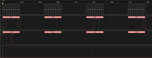
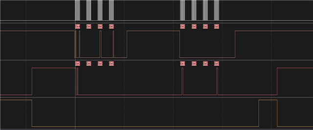
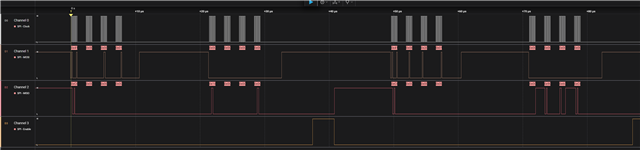
This is a snapshot of the SPI communication.

Any help would be nice.

Kind regards

  • Hi Thomas,

    Most initial SPI bring up issues are related to the chip select signal transitioning incorrectly relative to the data.  The clock to data polarity looks correct, but I can't see the full SPI transaction including the nCS signal. 

    The TCAN4550 requires the nCS signal transition Low at the start of the SPI Read/Write transaction and remain low until after the data portion is complete.  For a single register read/write, this means the nCS signal must be low for a total of 64 SCLK cycles (or 64 bits). 

    The device uses a FIFO on the SPI Interface to handle the SPI clock frequency to the OSC clock frequency domain crossing so it keeps track of how many bits are input and output from both sides of the FIFO. 

    On the SPI side, if there is an incorrect number of SPI clock cycles detected while the nCS signal is low, then there is either too few or too many bits in the FIFO which results in an error.

    Likewise if there is an issue with the OSC clock (crystal or single-ended CMOS clock of either 20MHz or 40MHz), then the digital core can't process the data resulting in errors. 

    Note that registers 0x0000 to 0x002F only require the SPI clock and are implemented in logic.  They are generally related to status information about the SPI FIFO interface.  But all other registers in the 0x0800 and 0x1000 domains require the OSC clock to be functional for a SPI read/write to be successful.

    Common things to check when getting initial SPI drivers running is that the nCS signal is low for exactly 64 clock cycles on a single register SPI read with Length field equal to 1.  By default a lot of MCU SPI driver functions set the nCS after every 8, 16, or 32 bits of data depending on how many bits it can process at a time. If nCS is pulled high before the correct number of cycles, this will cause the TCAN4550 to abort the SPI read and not provide the requested data on a read, or discard the data on a write to avoid corrupting the device with possibly invalid data.

    Also, the SCLK signal should be low while nCS transitions low at the start of the transaction to ensure the first SCLK edge is a rising edge. 

    Your clock to data phase relation already looks correct and data is sampled on the rising edge of SCLK.

    Can you capture the complete SPI transaction showing all 4 SPI signals including the nCS transitions?

    Regards,

    Jonathan

  • Dear Jonathan,

    Thank you for your reply.

    I checked if the nCS signal is low for 64 cycles. Here is the proof of that:


    I also checked if any of the interrupt enable flag registers on 0x0820 were able to be read, to rule out the OSC clock issue. I am able to read out the registers properly.


    Still, the initialization example code is not initialising properly, as the TCAN4550 will go to sleep after 3 minutes. 

       
       void Init_CAN(void){
       TCAN4x5x_Device_ClearSPIERR();                              // Clear any SPI ERR flags that might be set as a result of our pin mux changing during MCU startup
    
        /* Step one attempt to clear all interrupts */
    	TCAN4x5x_Device_Interrupt_Enable dev_ie = {0};				// Initialize to 0 to all bits are set to 0.
    	TCAN4x5x_Device_ConfigureInterruptEnable(&dev_ie);	        // Disable all non-MCAN related interrupts for simplicity
    
    	TCAN4x5x_Device_Interrupts dev_ir = {0};					// Setup a new MCAN IR object for easy interrupt checking
    	TCAN4x5x_Device_ReadInterrupts(&dev_ir);					// Request that the struct be updated with current DEVICE (not MCAN) interrupt values
    	
    
    	if (dev_ir.PWRON)                    
    	{                       // If the Power On interrupt flag is set
    		TCAN4x5x_Device_ClearInterrupts(&dev_ir);               // Clear it because if it's not cleared within ~4 minutes, it goes to sleep
    	}
    	/* Configure the CAN bus speeds */
    	TCAN4x5x_MCAN_Nominal_Timing_Simple TCANNomTiming = {0};	// 500k arbitration with a 40 MHz crystal ((40E6 / 2) / (32 + 8) = 500E3)
    	TCANNomTiming.NominalBitRatePrescaler = 2;
    	TCANNomTiming.NominalTqBeforeSamplePoint = 32;
    	TCANNomTiming.NominalTqAfterSamplePoint = 8;
    
    	TCAN4x5x_MCAN_Data_Timing_Simple TCANDataTiming = {0};		// 2 Mbps CAN FD with a 40 MHz crystal (40E6 / (15 + 5) = 2E6)
    	TCANDataTiming.DataBitRatePrescaler = 1;
    	TCANDataTiming.DataTqBeforeSamplePoint = 15;
    	TCANDataTiming.DataTqAfterSamplePoint = 5;
    
    	/* Configure the MCAN core settings */
    	TCAN4x5x_MCAN_CCCR_Config cccrConfig = {0};					// Remember to initialize to 0, or you'll get random garbage!
    	cccrConfig.FDOE = 1;										// CAN FD mode enable
    	cccrConfig.BRSE = 1;										// CAN FD Bit rate switch enable
    
    	/* Configure the default CAN packet filtering settings */
    	TCAN4x5x_MCAN_Global_Filter_Configuration gfc = {0};
    	gfc.RRFE = 1;                                               // Reject remote frames (TCAN4x5x doesn't support this)
    	gfc.RRFS = 1;                                               // Reject remote frames (TCAN4x5x doesn't support this)
    	gfc.ANFE = TCAN4x5x_GFC_ACCEPT_INTO_RXFIFO0;                // Default behavior if incoming message doesn't match a filter is to accept into RXFIO0 for extended ID messages (29 bit IDs)
    	gfc.ANFS = TCAN4x5x_GFC_ACCEPT_INTO_RXFIFO0;                // Default behavior if incoming message doesn't match a filter is to accept into RXFIO0 for standard ID messages (11 bit IDs)
    
    	/* ************************************************************************
    	 * In the next configuration block, we will set the MCAN core up to have:
    	 *   - 1 SID filter element
    	 *   - 1 XID Filter element
    	 *   - 5 RX FIFO 0 elements
    	 *   - RX FIFO 0 supports data payloads up to 64 bytes
    	 *   - RX FIFO 1 and RX Buffer will not have any elements, but we still set their data payload sizes, even though it's not required
    	 *   - No TX Event FIFOs
    	 *   - 2 Transmit buffers supporting up to 64 bytes of data payload
    	 */
    	TCAN4x5x_MRAM_Config MRAMConfiguration = {0};
    	MRAMConfiguration.SIDNumElements = 1;						// Standard ID number of elements, you MUST have a filter written to MRAM for each element defined
    	MRAMConfiguration.XIDNumElements = 1;						// Extended ID number of elements, you MUST have a filter written to MRAM for each element defined
    	MRAMConfiguration.Rx0NumElements = 5;						// RX0 Number of elements
    	MRAMConfiguration.Rx0ElementSize = MRAM_64_Byte_Data;		// RX0 data payload size
    	MRAMConfiguration.Rx1NumElements = 0;						// RX1 number of elements
    	MRAMConfiguration.Rx1ElementSize = MRAM_64_Byte_Data;		// RX1 data payload size
    	MRAMConfiguration.RxBufNumElements = 0;						// RX buffer number of elements
    	MRAMConfiguration.RxBufElementSize = MRAM_64_Byte_Data;		// RX buffer data payload size
    	MRAMConfiguration.TxEventFIFONumElements = 0;				// TX Event FIFO number of elements
    	MRAMConfiguration.TxBufferNumElements = 2;					// TX buffer number of elements
    	MRAMConfiguration.TxBufferElementSize = MRAM_64_Byte_Data;	// TX buffer data payload size
    
    
    	/* Configure the MCAN core with the settings above, the changes in this block are write protected registers,      *
    	 * so it makes the most sense to do them all at once, so we only unlock and lock once                             */
    
    	TCAN4x5x_MCAN_EnableProtectedRegisters();					// Start by making protected registers accessible
    	TCAN4x5x_MCAN_ConfigureCCCRRegister(&cccrConfig);			// Enable FD mode and Bit rate switching
    	TCAN4x5x_MCAN_ConfigureGlobalFilter(&gfc);                  // Configure the global filter configuration (Default CAN message behavior)
    	TCAN4x5x_MCAN_ConfigureNominalTiming_Simple(&TCANNomTiming);// Setup nominal/arbitration bit timing
    	TCAN4x5x_MCAN_ConfigureDataTiming_Simple(&TCANDataTiming);	// Setup CAN FD timing
    	TCAN4x5x_MRAM_Clear();										// Clear all of MRAM (Writes 0's to all of it)
    	TCAN4x5x_MRAM_Configure(&MRAMConfiguration);				// Set up the applicable registers related to MRAM configuration
    	TCAN4x5x_MCAN_DisableProtectedRegisters();					// Disable protected write and take device out of INIT mode
    
    
    	/* Set the interrupts we want to enable for MCAN */
    	TCAN4x5x_MCAN_Interrupt_Enable mcan_ie = {0};				// Remember to initialize to 0, or you'll get random garbage!
    	mcan_ie.RF0NE = 1;											// RX FIFO 0 new message interrupt enable
    
    	TCAN4x5x_MCAN_ConfigureInterruptEnable(&mcan_ie);			// Enable the appropriate registers
    
    
    	/* Setup filters, this filter will mark any message with ID 0x055 as a priority message */
    	TCAN4x5x_MCAN_SID_Filter SID_ID = {0};
    	SID_ID.SFT = TCAN4x5x_SID_SFT_CLASSIC;						// SFT: Standard filter type. Configured as a classic filter
    	SID_ID.SFEC = TCAN4x5x_SID_SFEC_PRIORITYSTORERX0;			// Standard filter element configuration, store it in RX fifo 0 as a priority message
    	SID_ID.SFID1 = 0x055;										// SFID1 (Classic mode Filter)
    	SID_ID.SFID2 = 0x7FF;										// SFID2 (Classic mode Mask)
    	TCAN4x5x_MCAN_WriteSIDFilter(0, &SID_ID);					// Write to the MRAM
    
    
    	/* Store ID 0x12345678 as a priority message */
    	TCAN4x5x_MCAN_XID_Filter XID_ID = {0};
    	XID_ID.EFT = TCAN4x5x_XID_EFT_CLASSIC;                      // EFT
    	XID_ID.EFEC = TCAN4x5x_XID_EFEC_PRIORITYSTORERX0;           // EFEC
    	XID_ID.EFID1 = 0x12345678;                                  // EFID1 (Classic mode filter)
    	XID_ID.EFID2 = 0x1FFFFFFF;                                  // EFID2 (Classic mode mask)
    	TCAN4x5x_MCAN_WriteXIDFilter(0, &XID_ID);                   // Write to the MRAM
    
    	/* Configure the TCAN4550 Non-CAN-related functions */
    	TCAN4x5x_DEV_CONFIG devConfig = {0};                        // Remember to initialize to 0, or you'll get random garbage!
    	devConfig.SWE_DIS = 0;                                      // Keep Sleep Wake Error Enabled (it's a disable bit, not an enable)
    	devConfig.DEVICE_RESET = 0;                                 // Not requesting a software reset
    	devConfig.WD_EN = 0;                                        // Watchdog disabled
    	devConfig.nWKRQ_CONFIG = 0;                                 // Mirror INH function (default)
    	devConfig.INH_DIS = 0;                                      // INH enabled (default)
    	devConfig.GPIO1_GPO_CONFIG = TCAN4x5x_DEV_CONFIG_GPO1_MCAN_INT1;    // MCAN nINT 1 (default)
    	devConfig.FAIL_SAFE_EN = 0;                                 // Failsafe disabled (default)
    	devConfig.GPIO1_CONFIG = TCAN4x5x_DEV_CONFIG_GPIO1_CONFIG_GPO;      // GPIO set as GPO (Default)
    	devConfig.WD_ACTION = TCAN4x5x_DEV_CONFIG_WDT_ACTION_nINT;  // Watchdog set an interrupt (default)
    	devConfig.WD_BIT_RESET = 0;                                 // Don't reset the watchdog
    	devConfig.nWKRQ_VOLTAGE = 0;                                // Set nWKRQ to internal voltage rail (default)
    	devConfig.GPO2_CONFIG = TCAN4x5x_DEV_CONFIG_GPO2_NO_ACTION; // GPO2 has no behavior (default)
    	devConfig.CLK_REF = 1;                                      // Input crystal is a 40 MHz crystal (default)
    	devConfig.WAKE_CONFIG = TCAN4x5x_DEV_CONFIG_WAKE_BOTH_EDGES;// Wake pin can be triggered by either edge (default)
    	TCAN4x5x_Device_Configure(&devConfig);                      // Configure the device with the above configuration
    
    	TCAN4x5x_Device_SetMode(TCAN4x5x_DEVICE_MODE_NORMAL);       // Set to normal mode, since configuration is done. This line turns on the transceiver
    
    	TCAN4x5x_MCAN_ClearInterruptsAll();                         // Resets all MCAN interrupts (does NOT include any SPIERR interrupts)
    	}


    Are there any other checks to do?

    Kind regards
    Thomas

  • Hi Thomas,

    I still see bit 3 of the Interrupts register 0x0820 getting set to 1 which is the SPI Error Bit (SPIERR). Can you read the Status Register 0x000C so that we can get more information about why the SPIERR bit is getting set?

    To prevent the device from entering Sleep Mode after 4 minutes, you simply need to write a '1' to the PWRON bit in the Interrupts register (0x0820[20]) or configure the MODE_SEL field in the Modes of Operation and Pin Configuration registers to "10" for Normal Mode (0x0800[7:6]).

    Can you try to simply read registers 0x0820, 0x000C and then write '1's to the set bits in each or just a blanket "0xFFFF" to both of these registers and read them back?  Any set bits should have been cleared.

    Please also try to write a custom value to the Test Register and Scratch pad and then read it back as a test that both the SPI Write and Read functions are correct.  You should read back the custom value you just wrote to this register.

    Can you also try to read back all of the device registers at the end of your configuration sequence into a log file so that we can compare the actual register values being written by the code and identify any errors?

    Regards,

    Jonathan