Other Parts Discussed in Thread: TCA9517A, TCA9517
Tool/software:
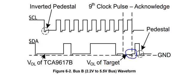
Under Section 6.3,
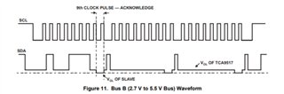
Analyzing the waveform of I2C bus on the B side, Things I can comprehend is -
1. Since ACK is done by B side (Vol of Target) so in this case A is Master sending the data to slave, B.
2. Blue Marked area in the circle, device on B releasing the data line and since the Buffer output is still ON the B stays on at SOV. once the Signal at the A rises above 0.3 of VCCA buffer turns OFF and the B line charges to VCCB.
Thing I am not able to understand is the inverted Pedestal, my thinking is like -
Device on B being the receiver which only reads the bus, until the 9th cycle it doesn't change anything on the bus and the Device on the A is Tx'er. When A goes low, Buffered output low is generated on B side which should be ~0.5V (SOV), Why does it go to 0V and then goes back to SOV level.
I also see the below image, which depicts the signal - A driving the B , Here I don't see B-side going to 0V and then moving to the offset voltage, which further confuses me.
Kindly Help me know what am I missing, explaining the logic behind that 0.
Regards,
Kiran