Part Number: TCA9534A
Tool/software:
Hi Team,
we using GPIO to simulate I2C to control the TCA9534A.
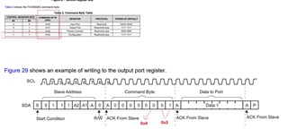
When I send I2C commands, such as I2C get unit 0 dev 14 reg 0x0, it works fine for the first four command after power on.
However, starting from the fifth command, I receive an error.
Is there a solution to this problem? or what is hte most likely problem? thanks for your help and learn from you.


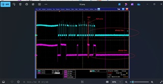
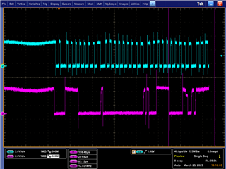 figure 01
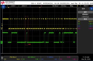
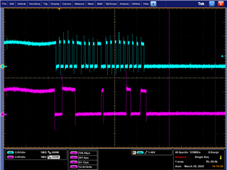 figure 02