This thread has been locked.

If you have a related question, please click the "Ask a related question" button in the top right corner. The newly created question will be automatically linked to this question.

TCAN4550-Q1: please review schematic

Part Number: TCAN4550-Q1
Other Parts Discussed in Thread: TCAN4550

Tool/software:

Dear team

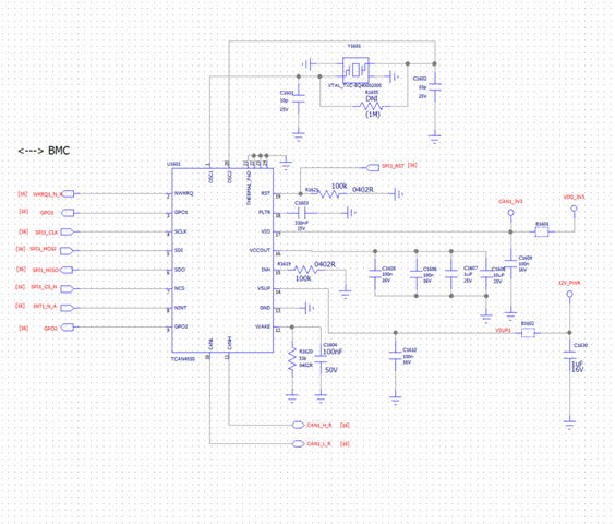
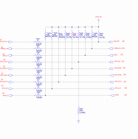
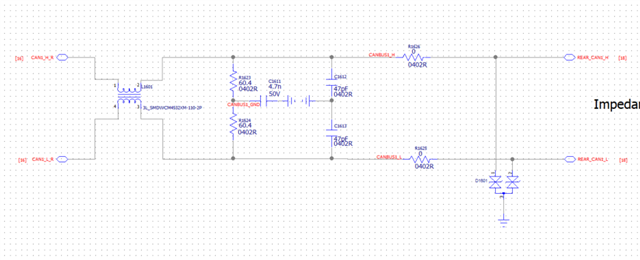
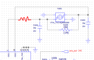
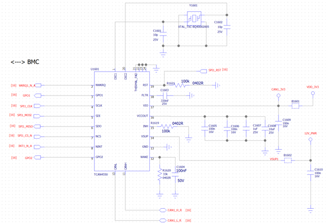
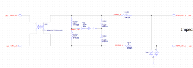
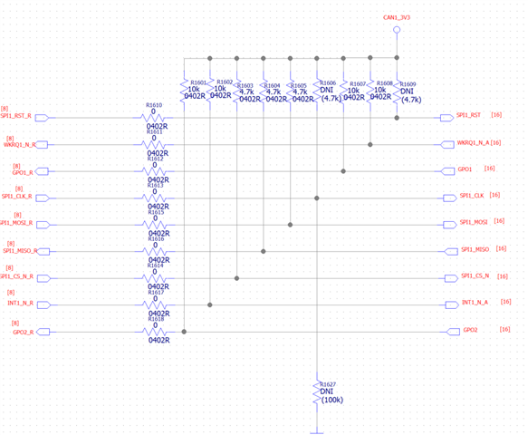
 we design in TCAN4550-Q1  in customer's new project.

Could you help to review the schematic?

thanks

  • Hello Jeremy,

    I have reviewed the schematic and have the following comments:

    • We recommend adding a series resistor between the OSC1 (pin 1) and the crystal to help optimizing the crystal performance for a stable clock.  See the TCAN455x Clock Optimization and Design Guidelines Application Report (Link) for more information.  A 0-ohm resistor can be used as a placeholder until it is determined a different value is required.
    • I would recommend having a decoupling capacitor on the TCAN4550 side of B1602 and placed as close to the device pin in the PCB layout.
    • The GPIO1 pin (labeled GPO1 in the schematic) is an output pin that is driven to either VIO, or GND and does not require a pull-up resistor. 
    • The nWKRQ pin is configurable, but by default will output 3.6V when the device is in Sleep Mode that is derived from an internal supply.  If a pull-up resistor is used on this pin, the register configuration should configure this pin to be an open-drain so that if the VDD_3V3 supply is disabled during sleep mode, the nWKRQ doesn't back drive this supply with 3.6V.
    • Pull-up resistors are generally not recommended for the clock and data lines (SCLK, SDO or MISO, and SDI or MOSI).  These may need to be DNI if there are communication issues.

    Regards,

    Jonathan

  • HI Johnathan , 

    Is GPO2 need pull up 3.3V ?

    and update schematic , 

    thanks

  • Hi Jeremy,

    Is GPO2 need pull up 3.3V ?

    Yes.  See the description in the datasheet.

    For the recommendation of the series resistor between the OSC1 pin and the crystal, I was not talking about a 1M resistor between OSC1 and OSC2 pins.  The TCAN4550-Q1 already has an internal 500k resistor between OSC1 and OSC2.  Instead I was talking about a series resistor located directly between the OSC1 pin and the load cap and crystal.  The purpose of this resistor is to help reduce the amount of current flowing through the crystal and reduce the Drive Level or power dissipation if necessary. 

    Regards,

    Jonathan