This thread has been locked.

If you have a related question, please click the "Ask a related question" button in the top right corner. The newly created question will be automatically linked to this question.

THVD9491-SEP: Slew Rate Pin issue

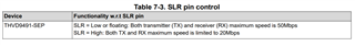
Part Number: THVD9491-SEP

Tool/software:

Hello

I am inquiring if I can receive the internal circuit diagram of THVD9491-SEP (RS-485 Transceiver).

Currently, I have designed the circuit for THVD9491-SEP as follows. (Instead of the actual full circuit, I'm replacing it with a simplified image of just the power section)

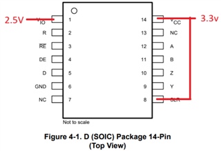
As you can see in the image, I've connected the SLR pin to the 3.3V VCC pin, and VIO is 2.5V.

The input voltage allowable range for the SLR pin is -0.3 < SLR < 2.7V (VIO+0.2).

Because I've exceeded the input voltage allowable range, it would be correct to change the design, but after checking the datasheet, I found out that the input voltage allowable range for the VIO pin is -0.5 < VIO < 3.5V (VCC+0.2).

Based on the situation, it seems that even if up to 3.7V is input to the SLR pin, there shouldn't be a major issue.

For this reason, I would like to request information about the chip's internal circuit to review whether there would be any issues with chip operation without changing the design.

Or if it's not possible, please let me know if it's not a big deal for the SLR Pin to be connected to 3.3V while VIO is 2.5V.

Sincerely,

MS Kim

  • Hi MS Kim,

    Thanks for reaching out on E2E about this question! I understand the dilemma that you are in. 

    Unfortunately, we cannot share the internal diagram as it is private TI intellectual property.

    You are correct that VIO has an absolute max up to VCC + 0.2 (3.5V in your case). However, since SLR is internally referenced to VIO, this SLR voltage difference can leak onto the VIO pin (i.e. 3.3V rail leaking onto the 2.5V rail through SLR). This has the potential to interfere with other components in a system, particularly to disrupt LDOs if it cannot regulate VIO correctly. This is why the input voltage abs max is VIO + 0.2, and we just cannot recommend ignoring this specification. 

    Because of this, the best path forward here would be to change the design so SLR is referenced to the correct voltage (2.5V). I know this is not the answer you were hoping for, but hopefully that provides some clarification. If you have any other questions, don't hesitate to reach out.

    Best regards,

    Ethan

  • Thanks for the reply. I have an additional question.

    The PCB already came out with that circuit(SLR Pin connected to 3.3V VCC).

    So I'm planning to physically cut the PCB trace between SLR Pin and 3.3V VCC.

    Is cutting the trace between the SLR pin and the 3.3V VCC pin to make SLR Pin floating completely identical to connecting the SLR pin to the 2.5V VIO pin in terms of chip's stability?

    What I'm concerned about is that make SLR Pin floating will have any negative impact on the chip's performance or the chip itself.

  • Happy to help MS Kim.

    Leaving SLR floating will keep the device operating at its max data rate of 50Mbps:

    Cutting the trace so it is floating is just fine. Tying it high would limit the device to 20 Mbps. 

    If you have any other questions, just let us know!

    -Ethan