This thread has been locked.

If you have a related question, please click the "Ask a related question" button in the top right corner. The newly created question will be automatically linked to this question.

TUSB217A-Q1: DP/DM internal or external bypass?

Part Number: TUSB217A-Q1

Tool/software:

Hi,

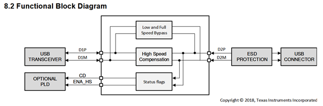
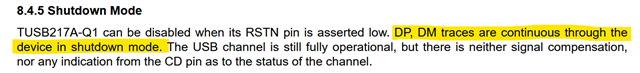
I am confused about the proper connection of the USB data pairs to TUSB217A-Q1. The 8.2 block diagram and statements in paragraph 8.4.5 lead me to believe there is an internal bypass for the D1P/M pairs.

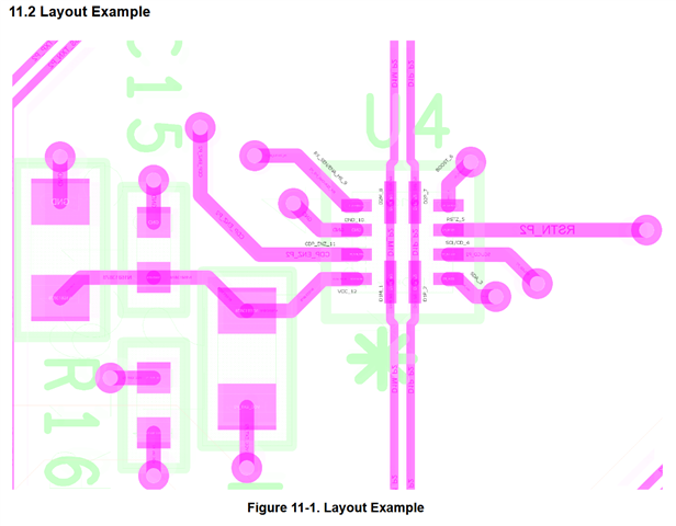
But, when I look at the layout example, I see PCB traces shorting pads 1/8, and 2/7. I can't find an explicit statement in the datasheet that calls for a short of the pads on the PCB.

What is required?

Thanks!

  • Hi Zoltan,

    For the TUSB217A-Q1, the DP/DM lanes needs to stay connected underneath the device. If these are not connected, the USB2 lines will be broken, and will be inoperable.

    Please let me know if you have any other questions.

    Thanks,

    Ryan