This thread has been locked.

If you have a related question, please click the "Ask a related question" button in the top right corner. The newly created question will be automatically linked to this question.

AM26C32: The impedance of one of the differential input terminals (A, B) is abnormally low.

Part Number: AM26C32

Tool/software:

Thank you for your help.
I'm in trouble.

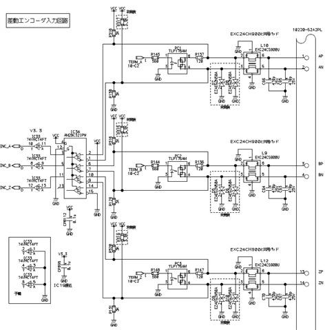
I have developed a control device for a two-phase stepping motor.

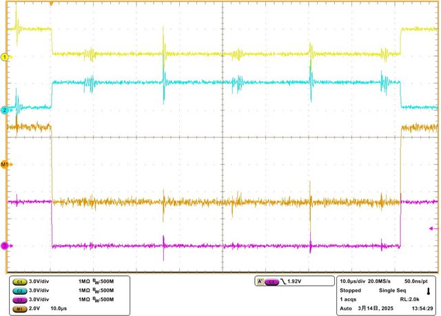
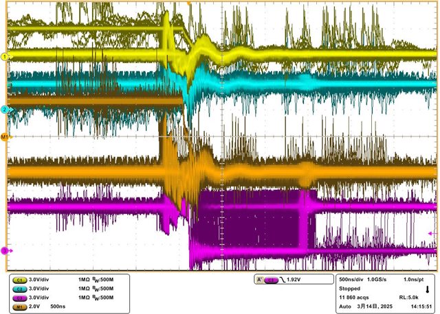
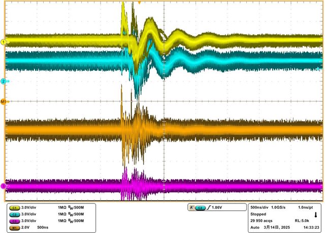
The two-phase stepping motor has an A/B phase output encoder (RS422 driver output).
The output of that encoder is input to the control device I developed.
I am using a line receiver: AM26C32IPW for the input part.

However, it has broken down over time.
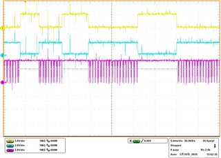
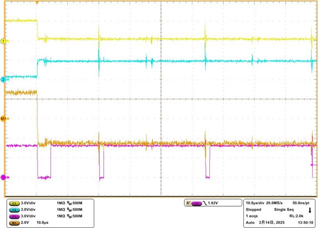
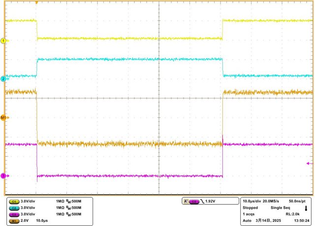
The output of the differential input result is abnormal.
I have not been able to identify the cause.

When I removed the broken AM26C32IPW from the board and examined it, I found that the impedance of only one of the input terminals was abnormally small.
The table below shows the results of measuring the impedance between VCC and the input terminal, and between GND and the input terminal.

Pin Signal          VCC        GND
-------------------------------------------------------------------------------
1A Phase A +    252kΩ      3.2MΩ
1B Phase A -     3.2MΩ     250kΩ
2A Phase B +    252kΩ     3.2MΩ
2B Phase B -     2.9MΩ    0.57kΩ
3A Phase Z +     252kΩ    3.2MΩ
3B Phase Z -     3 2MΩ    252kΩ
4A Unused         -             -
4B Unused         -             -
-------------------------------------------------------------------------------

Only the impedance between the pin 2B and GND is low (0.57kΩ).

This failure occurs in multiple devices.
However, it occurs randomly in phases A, B, and Z.
What do you think is the cause of this failure mode?

Thank you in advance.

  • A photo of the installed state is attached.

  • The device can be damaged when you exceed the absolute maximum ratings.

    Can voltages below −11 V or above 14 V happen? Are there any protection components?

  • Thank you for your response.

    The AM26C32 is powered by a +5VDC power supply.

    A Common Mode filter (type:EXC24CS900U [Panasonic]) with a built-in surge protection element has been inserted in the differential power line of the AM26C32.

    I have attached a reference waveform.

    I have attached the waveform.
    CH1: Input 2A (+)
    CH2: Input 2B (-)
    CH3: Output

    Thank you in advance.

  • Please show the schematic.

    ESD protection does not help against slower transients with a lower voltage.

    The A and B signals are very noisy, and the common-mode choke will filter out only common-mode noise. Please tell the oscilloscope to compute A−B.

    The input waveforms shown are OK, but I can imagine that there are sometimes voltage spikes that exceed the absolute maximum ratings. If the encoder and your device share a ground (i.e., there is no offset between their grounds), then you can simply add diode clamping to the 0 V/5 V power rails. And low-pass filters might help.

  • As Clemens pointed out, seeing a schematic would be helpful here.

    Is there any kind of hot plug event occurring? 

    How long does it usually take for the pins to break? 

    Are you doing surge testing on the lines?

    -Bobby

  • Dear Clemens

    Thank you for your opinion.

    I have one concern.

    The problem is with the feedback encoder signal, but due to the structure of the device, there is a part where it is bundled with the PWM signal line for the motor drive (about 300 mm) and there is a situation where the signal is crosstalking.

    There is no cable shielding in that part.

  • Dear BOBBY

    Thank you.

    I have attached the circuit diagram.

    EZAEG2N50A(Panasonic) is not implemented.

    Would it be better to also add a normal mode filter?

  • The filter may help with some of the noise but I'm not sure if that noise is real (being picked up by the probe through the air)... 

    I don't see anything here that would indicate the device breaking. 

    Any idea how long it takes for a device to break?

    Have you tried populating the bidirectional TVS and seeing if any devices break? If the Bidirectional TVS work, it probably means the damage was coming from a fast transient event occurring. If it still breaks after the external bidirectional diode being present then I think the damage is from a slower transient event similar to a surge event. 

    If the damage is coming from an over voltage event, you could try implementing this TI design below. I would try populating the bidirectional TVS diodes first though.  

    https://www.ti.com/lit/ug/tiduer9/tiduer9.pdf?ts=1744061146358&ref_url=https%253A%252F%252Fwww.google.com%252F

    -Bobby

  • Dear BOBBY,

    Thank you for your reply.

    There may be something we should check before taking drastic measures.

    It takes some time for the equipment to break down like this.

    However, since this is an issue that is occurring at our user's site, we are currently checking but are unable to grasp the details.

    There are multiple units of this equipment stored in the storage panel, but this is one specific unit. Even after replacing it with a normal unit, the replacement unit broke down in the same place again.

    We are currently considering re-testing the lightning surge.

    We will consider the TI design you proposed (TVS diode + PTC fuse) in the future.

    Thank you.

  • Hi Toshikazu,

    Let me know if you find out any additional information. Maybe you can probe the A/B pins and set the o-scope to trigger outside of the abs max (+/-14V). 

    It could be possible that maybe the noise coupling onto the pins exceed this rating for a small amount of time and slowly damage the device. If that is what's happening then the TVS diodes you have should help clamp it. Might be worth populating and seeing if the damage occurs after it's populated.

    -Bobby

  • Dear BOBBY,

    Thank you for your suggestion.

    I am attaching the waveforms that we are currently verifying in-house.

    ■Measurement points
    CH1: 1B (Receiver input +)
    CH2: 2B (Receiver output -)
    CH3: ENC_B (Receiver output)
    M1: CH1-CH2 (Differential calculation result)

    ■Measurement waveform
    91 Servo ON at amplifier ④
    92 Servo OFF at amplifier ④
    93 Servo ON at amplifier ①
    94 Servo ON at amplifier ④ (overwriting)
    95 Servo ON at amplifier ① (overwriting)
    *Amplifier ① is a normal device
    *Amplifier ④ is a B-phase abnormal device

    No.91

    No.92

    No.93

    No.94

    No.95

    Thank you in advance.

  • Dear BOBBY,

    sSorry, the text may not be displayed properly,
    so I will explain the following points again.

    ■Measured waveform
    91 Servo ON at amplifier No. 2
    92 Servo OFF at amplifier No. 2
    93 Servo ON at amplifier No. 1
    94 Servo ON at amplifier No. 2 (overlapping)
    95 Servo ON at amplifier No. 1 (overlapping)
    *Amplifier No. 1 is a normal device
    *Amplifier No. 2 is a B-phase abnormal device

    Thank you in advance.

  • No.91

    None of these signals look like they are going outside of the abs max. 

    A-B looks relatively clean. I do find it strange that the CH3 is toggling. I'm wondering if the R output is probed at the wrong channel. Since A-B is negative we expect R to be a logic low for the entire duration of the signal.

    No.92

    This looks good, exactly what I would expect.

    No.92

    No issue with this one as well.

    No.93

    More noise but overall looks okay since A-B doesn't see much of it and R output remains stable.

    No.94

    This one, you may wanna double check the max/min values you see on the A/B pins to see if they exceed the abs max. I don't necessarily see it but with it zoomed out we may not catch it. 

    No.95

    94 vs 95, there seems like a lot more distortion/noise is appearing. Is 94 the confirmed broken unit? 

    -Bobby

  • Dear BOBBY,

    Thank you for checking the waveforms.

    These waveforms were taken in our development lab.

    They are not from the user's equipment environment where the problem is occurring.

    Even if it were possible to take them, it would be impossible because there are no probe points due to the cable and equipment structure.

    No. 94 is the waveform of a broken unit.

    CH.3 output returns to its original state immediately after switching (failure mode).

    Is it the absolute maximum rating of the receiver IC after all?

    It will take a while, but I will try to take a waveform again using the absolute maximum rating as a trigger.

    These noise disturbances are waveforms affected by the motor PWM signal after the motor control servo is turned on.

    Looking at No. 94 and No. 95 (motor control servo ON), the PEEK appears to be about +/-6V at the moment it is affected by the noise.

    However, the PEEK appears to be for a very short period of time (about 20ns to 30ns?).
    Even so, is there a good chance that the receiver IC will be damaged?

    I will try to collect the waveform again using the absolute maximum rating as a trigger.

    I am currently re-running various noise tests at the same time.
    As of yesterday, I conducted a static electricity test (IEC 61000-4-2) at 8.8kV and confirmed that there were no problems.
    Today I will conduct a lightning surge test (IEC 61000-4-5) from +/-1kV, prepared to damage the equipment.
    I will gradually increase the surge voltage from +/-1kV until it breaks.

    Thank you for your support.

  • Is it the absolute maximum rating of the receiver IC after all?

    Usually when you break the abs max rating, it completely breaks the pin with either a short to adjacent or Vcc/GND. This kind of looks like it's somewhat operational. So I don't immediately know if it's some kind of short duration damage that occurred (like a transient that occurs in nanosecond range) or if something else is going on here.

    These noise disturbances are waveforms affected by the motor PWM signal after the motor control servo is turned on.

    Yeah I figured as much, anytime theres motor's turning on and off I usually expect noise being emitted through air or through PCB capacitive coupling occurring. 

    However, the PEEK appears to be for a very short period of time (about 20ns to 30ns?).
    Even so, is there a good chance that the receiver IC will be damaged?

    The problem is, I don't know if the waveforms we're seeing are from the probe picking it up through the air (which would give fake waveform noise) or if the pins are actually seeing this. The TVS diode you have a spot for should help clamp that noise since those usually can trigger within nanoseconds. 

    Today I will conduct a lightning surge test (IEC 61000-4-5) from +/-1kV, prepared to damage the equipment.
    I will gradually increase the surge voltage from +/-1kV until it breaks.

    This device isn't rated for surge and I don't see much external surge protection on the schematic for the A/B pins so my guess is 1kV would probably break the device. The TVS diodes probably won't  be able to handle it if that's the only protection against surge. 

    -Bobby

  • Dear BOBBY,

    Thank you for all your advice.

    I conducted a lightning surge test.

    The surge was applied to the motor control line + encoder feedback line (3m section).

    It withstood 1kV.

    It broke down at 2kV.

    First, I confirmed that a surge of this level could cause a breakdown.

    In the end, I recognize that the problem is that something similar to this is happening in the user's equipment.

    Even so, we must investigate the process that led to the breakdown.

    What I'm concerned about now is that the device equipped with the receiver (AMP) and the device equipped with the motor + encoder (DRV) are connected by a 3m cable.

    Power to the encoder is supplied via the power line in this cable.

    If a lightning surge is applied to the AMP, how will this affect the GND and VCC potentials of the AMP and DRV?

    Even if it's only about 3m long, will the VCC and GND potentials on the DRV side, which are connected by thin signal wires, not be disturbed between the AMP and the AMP?

  • Hi Toshikazu,

    Sorry for the late response (I've been out of office). 

    I suspect with such large power dissipation during a surge event, if the GND plane isn't large enough it could result in a GND shift on the AMP side for a moment of time. Though, some of the charge would probably also flow into the DRV side of the GND as the AMP GND shifts up. The severity of the shift up is something I'm not entirely sure we would know without probing the two GNDs during the surge event. 

    As for Vcc, if you have external surge protection, I would assume the current will flow into the diodes to GND when the diodes begin to clamp the surge. This may require additional diodes/protection on the DRV side on the Vcc line. 

    -Bobby

  • Dear BOBBY,

    Thank you for your reply.

    I simulated a model of the AMP and DRV sections connected with a 3m cable, in which a single-mode 0.5kV/1.2us surge is injected into the AMP power supply.

    AMP circuit impedance: 33Ω (R1).
    DRV circuit impedance: 33Ω (R2).
    3m cable +/- power line model: 0.2Ω・5.3uH
    Signal source impedance: 2Ω

    Each measurement value is based on GND.
    The DRV side (R2) is floating at the end of the cable.

    The model is very simple, but as the light blue measurement shows, there is a tendency for it to bounce against the GND reference.

  • The output impedance of the signal source looks like it may be out of the surge spec if I recall correctly. I think the coupling element is supposed to be around 40 ohms (80 ohms in parallel with each other for a symmetrical set up). 

    From the IEC standard:

    TI's set up for testing surge: (80//80= 40 ohms as per standard)

    What do R1 and R2 represent in the schematic? Is this the impedance of the external diodes? 

    There are also some capacitances to GND due to board parasitics and parasitics from device pin/bond wires that you could add in the simulation. Maybe around 50pF on both sides of the 33 ohm resistors. 

    I don't think those negative bounces will exist in the real system with diodes on the boards though they could break during the surge events. 

    -Bobby

  • Hi BOBBY,

    Thank you for showing us the IEC test environment.

    The simulation results shown here are R1 equivalent to an AMP device (assuming a load of 33 Ω), and R2 equivalent to a DRV device (assuming a load of 33 Ω).

    Power is being supplied to these devices (R2 is supplied via a 3m cable).

    The simulation was performed on the case where a single-mode (power + side only) surge was applied to this power supply.

    This simulation does not take into account the RS-485 communication system.

    We looked at how it affects the GND between R1 and R2.

    That's all about the simulation.

    After that, we conducted tests to add static electricity to the RS-485 signal line. Now, we are experiencing a phenomenon where the RS-485 receiver on the AMP device is failing, and we are verifying this through tests based on the possibility that static electricity may have entered from the RS-485 transmitter side of the DRV device. We are considering the possibility that the DRV device equipped with an RS-485 transmitter is charged. The failure was reproduced by applying static electricity equivalent to 13kV to the signal terminal of the RS-485 transmitter (air discharge).

    Currently, the tests that have been used to reproduce the failure are as follows:

    (1) Lightning surge (IEC61000-4-5) 2kV to the RS-485 signal cable

    (2) Static electricity (IEC61000-4-2) 13kV to the signal terminal of the RS-485 transmitter

    The problematic device is operated in a line of several dozen units in close proximity at the site, and occasionally (about once every two weeks) one of them breaks down. However, for some reason, it is one unit in a specific location.

  • Hi Toshikazu,

    Thanks for clarifying. Looks like I misunderstood on the where you were testing this surge (RS485 side was what I was thinking). If so, the 33 ohm resistors make more sense now. 

    The problematic device is operated in a line of several dozen units in close proximity at the site, and occasionally (about once every two weeks) one of them breaks down. However, for some reason, it is one unit in a specific location.

    If we're thinking the device is getting damaged through air discharge, it may help to add a series resistor of around 10 to 20 ohms (pulse proof) and populating the TVS diodes which should help if it's air discharge. If the specific unit isn't getting damaged after populating the TVS and adding a series resistor after a month+, it would probably confirm the issue was air discharge. Though I understand trying to test this through out a month+ timeframe may not be the best approach if there are time constraints. 

    -Bobby

  • Hi BOBBY,

    Thanks for all your advice.

    Yes, it seems that adding a small resistive load in series can suppress di/dt. It's difficult to actually do this at the moment, but I'd like to understand that it's a possible solution along with TVS.

    Thank you.

    As this is an issue occurring at a user's facility, we're having difficulty dealing with it, but we'll take your advice as a hint for a solution.

    I think it will take some time to resolve.

    Thank you for all your support.
    We will continue to work on it.