


Part Number: SN55LVCP22A-SP
Tool/software:
Hi,
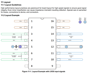
On page 20 (section 11) of the SN55LVCP22A-SP datasheet, there is a layout example for this part. I was wondering if there was any significance to the lengths of the traces for each pin according to the image in Figure 11-1? Such as SEL1 (pin1) being half the length of IN0+ (pin3) in that image, Figure 11-1?
In regards to the footprint for this, due to the Ceramic Flatback package, we will need to have this part lead-formed, so we are currently in the process of generating this part's footprint and lead-form profile. We are now confused as to the sizes of the pads because the image below (figure 11-1) shows pins 3, 4, 6, 7, 10, 11, 12, 13 & 14 being longer than the other pads.
Is Figure 11-1 just a representation of the layout and does not represent the actual size of the traces? Is it recommended that all the pads for this footprint be the same length/size?
Would there happen to be an example of this part's lead-forming profile that can be provided?
Thanks,
Tristan

