


Hi,
From TXS0102 webpage one could download symbol and footprint for YZP package. However, I found that the schematic symbol converted from Orcad v9.x format, show different pin assignment from the datasheet.
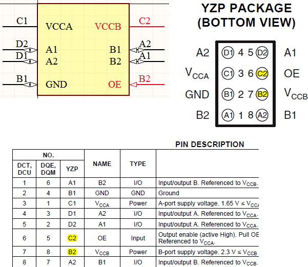
The difference is with VCCB and OE pins. The way they are mapped to C2, B2 pins are opposite between the schematic symbol and the datasheet.
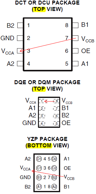
In addition, there are also symmetries and asymmetries between of pin mapping in different packages. Naturally, one would think of (VCCA, VCCB) being a pair and expect their geometry to also exhibit such symmetry. This is the case of DQE and DQM package, in which we see [pin 1, VCCA] and [pin 8, VCCB] are on the opposite sides of the chip.
However, in {DCT, DCU} and YZP package, although VCCA and VCCB are on the opposite sides, they are displaced by one position. But, since I have observed opposite configuration in datasheet and Orcad symbol of YZP package, this also raises doubts to the correctness of drawing in the datasheet.
Could TI employee confirm which of the datasheet and the Orcad schematic is correct?
Tim


