This thread has been locked.

If you have a related question, please click the "Ask a related question" button in the top right corner. The newly created question will be automatically linked to this question.

SN65LVCP22: Unexpected Output Behavior During SEL Switching in

Guru 12155 points
Part Number: SN65LVCP22

Tool/software:

Hi,

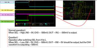
We are currently evaluating the SN65LVCP22 used as a 2:1 LVDS crosspoint switch in our system, and have observed unexpected output voltage behavior during SEL switching.

Configuration:

  • Device: SN65LVCP22

  • Usage: 2:1 LVDS switch (IN0 or IN1 to OUT based on SEL)

  • SEL = High: IN1 → OUT

  • SEL = Low: IN0 → OUT

  • Both IN0 and IN1 receive AC-coupled LVDS signals from other devices.

Observed Issue:
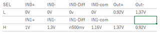
When switching SEL from High to Low to route IN0 to the output, we observe +500mV at the output even though IN0 is at 0V (no signal).
However, when both IN0 and IN1 are at -500mV, switching SEL results in the expected -500mV at the output.

Our Understanding:
We believe this behavior is not a device failure, but may relate to one of the following:

  1. IN0 may be in a High-Z state during SEL transition, and the output reflects an internal bias voltage (~+500mV).

  2. The device may produce undefined output voltage if switching occurs while the input is not actively driven.

  3. Lack of termination or pull-down on a floating input might be causing this behavior.

We would appreciate it if you could advise whether this output behavior is expected under the above conditions, and whether there are any recommended countermeasures (e.g., input biasing, termination guidance, or switching timing considerations).

Thanks,

Conor

  • Hi,

    Just checking in to see if there has been any progress on this topic since our last reply.
    If there are any updates, please let us know.

  • HI Conor:

       Sorry for late response, this device was just assigned to our group.

        when switching SEL from high to low, do you mean both SEL0/SEl1 switching from high to low?

    Regards

     Brian

  • Hi Brian,

    Thank you for your reply.

    when switching SEL from high to low, do you mean both SEL0/SEl1 switching from high to low?

    • In our configuration, the SN65LVCP22 is used in the "1:2 splitter" mode, and as such, the same control signal is applied to both SEL0 and SEL1 pins.

    • When SEL0 and SEL1 are switched from High to Low, the internal logic is expected to switch the output connection from IN1 to IN0 accordingly.

    • However, we are observing the following behavior during actual operation:

      - When IN0 = 0V and IN1 = -500mV, switching SEL0/SEL1 from High to Low should ideally result in Vout = 0V, but we instead observe Vout = +500mV.

      - On the other hand, when IN0 = IN1 = -500mV, switching SEL0/SEL1 results in Vout = -500mV, which is the expected behavior.

    As SN65LVCP22 is designed for AC-coupled differential input with internal biasing, if one side of the input differential pair is fixed to 0V while the other is left floating (not connected), the internal bias may pull the floating pin to an intermediate level (e.g., ~+500mV). As a result, the device may interpret this as a +500mV differential input and incorrectly drive a +500mV differential output. 

    We understand that this is an unintended use case, but we would appreciate your insight on whether such behavior is plausible given the internal receiver bias structure. If there are any recommended mitigation techniques (e.g., always terminate inputs with 100Ω, ensure differential input is valid before SEL switching), we would greatly appreciate your suggestions.

    Thanks,

    Conor

  • HI Conor:

    1: if you send any AC signal to IN0 and IN1, dies device working as expected?

    2:for IN signal, min DC common mode volatge is 50mv, so 0v DC is out of datasheet spec..

    Best

    Brian

  • Hi Brian,

    1. No, the input voltage is a DC signal.

    2. Are the following input ranges outside the operating range? 

    - On the other hand, when IN0 = IN1 = -500mV, switching SEL0/SEL1 results in Vout = -500mV, which is the expected behavior.

    Thanks,

    Conor

  • IN0 /IN1 in scope is single ended or differential signal?

    IN0  seems  0v., is it?

    Regards

    Brian

  • Hi Brian,

    IN0/IN1 on CH1 and 3 are differential signals. As you know, IN0 is 0V.

    The image contained some Japanese text, so I am sending you the corrected version again.

    As stated in the image, what we would like to know is, "When SEL = Low, IN0 = 0V, CH3 = -500mV, OUT = IN0 = 0V should be output, but why is the CH4 waveform outputting +500mV?" Please answer, including whether this behavior is expected of the IC.

    Thanks,

    Conor

  • Hi Conor:

    Can you look at single ended signal and fill in the form below?

    SEL IN0+ IN0- IN0-Diff IN0-com Out+ Out-
    L     0v      
      IN1+ IN1- IN1-Diff IN1-com    
    H     n500mv      

    Regards

    Brian

  • Hi Brian,

    I have entered the information below, could you please check it?

    Thanks,

    Conor

  • HI Conor:

       Assume OUT0 and OUT1 are same

          Can you make a little difference between IN0+ and IN0- (like IN0+ is 100mv, IN0- is 0v)? so it will make it easy to see if mux works correct or not.

          From above table, when SEL is high, OUT+ should be 0.92v and OUT- should be 1.37V.

    Best

    Brian

  • Hi Brian,

    Thank you for your reply.
    Before checking, please confirm the following points.

      Can you make a little difference between IN0+ and IN0- (like IN0+ is 100mv, IN0- is 0v)? so it will make it easy to see if mux works correct or not.

          From above table, when SEL is high, OUT+ should be 0.92v and OUT- should be 1.37V.

    When the IN0 differential input is 0V (IN0+ = 0V, IN0− = 0V), the device may interpret this as no active differential input, which could result in unstable or undefined output levels — potentially drifting toward the internal bias point (e.g., around +500mV).
    This makes it difficult to confirm whether the output is correctly reflecting the selected input after SEL transitions.
    Therefore, by introducing a small voltage difference between IN0+ and IN0−, it becomes easier to visually confirm whether the output is switching correctly to the expected input.

    Could you please confirm if our interpretation is correct?

  • Your interpretation is correct.

    Best

    Brian