This thread has been locked.

If you have a related question, please click the "Ask a related question" button in the top right corner. The newly created question will be automatically linked to this question.

SN65DPHY440SS: no MIPI CSI output when input waveform is there

Part Number: SN65DPHY440SS


Tool/software:

Hi,

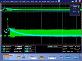
I am designing a camera board with a 300mm long FPC. Considering length of the FPC, a SN65DPHY440SS is added. When PCB and FPC are back, I found no MIPI CSI transmission at all. During debug, I can see MIPI CSI signals on input side of SN65 BUT no output waveform at all. See below waveform, the green signals which is measured at input port of SN65 IC, LP and HS signals can be identified. But the blue one, which is measured at output side of IC, HS signal is almost zero.

Another test was also performed by removing the SN65 IC and directly connecting input pad and output pad on PCB. MIPI CSI was working good then. 

Could you please help to provide some ideas on this? Thx a lot in advance.

  • Hi,

    Are you able to share the schematic? I can review this to see whether there in an implementation issue.

    Have you tried multiple SN65DP440SS devices or do you only see this issue on one unit?

    Best,

    Shane

  • Actually, there is nothing specially here, CSI input from camera to SN65DPHY and expect output from retimer to SOC. SN65DPHY is powered by a 1.8V power rail. We have 10 boards with same issue. We tried to remove the ICs and blue-wired the input/output pad on PCB in 2 of these boards and CSI transmission can both be fixed 

  • For the schematic RSTN should have a 200nF capacitor to GND. Otherwise the implementation looks ok from what is shown. To be sure, can you check that your powerup sequence fits the datasheet requirements?

    Are you able to reset the device by driving RSTN low after power-up? This would help determine if the RSTN signal is the problem.

    Best,

    Shane

  • Hi Shane,

    Thx for the feedback. I will replace the RSTN cap and try to reset IC by pulling it down.

    As for the power up sequence, in this design, RSTN is NOT controlled, so, there is no power up sequence to-be-controlled.

    Besides, I also noticed another parameter in datasheet, 'differential input common-mode voltage HS Receive mode, V(cm_rx).which define as min.70mV and max.330mV. My question is, if the input voltage exceeds the max. value (GREEN input HS signal seems to be marginal), will it trigger any protection protocol and then IC shut itself down?


  • RSTN is NOT controlled, so, there is no power up sequence to-be-controlled.

    You can adjust the rise time on RSTN by changing the capacitor value to GND without actually controlling the signal. The idea is to slow the rise on RSTN so it fits the td1 spec.

    if the input voltage exceeds the max. value (GREEN input HS signal seems to be marginal), will it trigger any protection protocol and then IC shut itself down?

    If the HS signal voltage exceeds the maximum, the device may revert back to LP mode. This would kill any high speed transmission on the TX side. 

    Another thing to check: is the clock signal present on DACP/N when running this test?

    Best,

    Shane