This thread has been locked.

If you have a related question, please click the "Ask a related question" button in the top right corner. The newly created question will be automatically linked to this question.

DS90CF364: RxIN0 to RxOUT delay time

Part Number: DS90CF364

Tool/software:

Hello team,

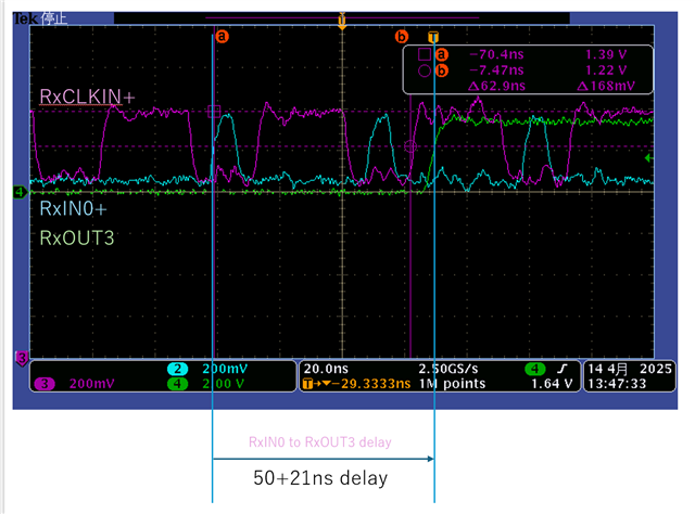
My customer would like to clarify the RxIN0 to RxOUT delay time of DS90CF364.

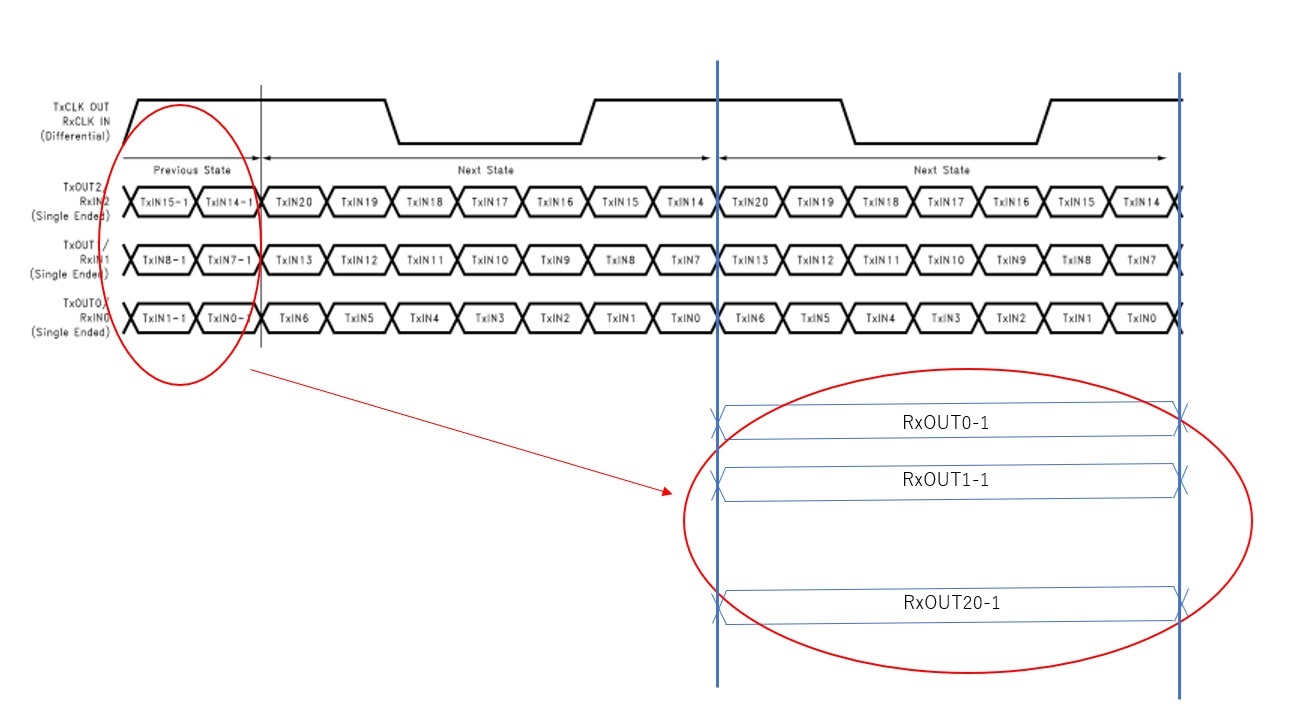
The customer uses 20MH clock for RxCLK. They measured the delay time is the following.

RxIN0 to RxOUT0 delay time : 50ns (1cycle)
RxIN0 to RxOUT3 delay time : 50ns+21ns 

The waveform is the following.
/cfs-file/__key/communityserver-discussions-components-files/138/DS90CF364_5F00_waveform.pptx

Is This delay time appropriate?  Also I and the customer do not know it from the datasheet of DS90CF364, so would you please advise where this delay is described in the datasheet?

Your advice is appreciated.

Best Regards,
Akihisa Tamazaki

  • Hi Akihisa,

    The DS90CF364 is a LVDS receiver converts LVDS input to CMOS/TTLRGB parallel output.

    So the inputs are LVDS data in 3 data lanes (RxIN0/1/2) and one clock lane RxCLK IN.
    The outputs are in RxOUT (6 Red, 6 Green, 6 Blue, and 3 control lines) and clock output RxCLK OUT.


    The delay between RxCLK IN and RxCLK out is "RCCD" in the "Receiver Switching Characteristics" table. Also shown in Figure 13. It should be between 5.0 to 9.0 ns.


    Since the LVDS interface format and TTL/ RGB interface are different, RxIN0 to RxOUT0/3 are not directly correlated and would depend on the pixel color being transmitted in that instance. These are different data formats, and the LVDS format mapping is shown here:


    Best regards,
    Ikram


  • Ikram-san,

    Thank you for your support.

    However, the customer wants to know this delay to design FPGA code and asks an additional question. It can be seen from the measurement waveform so that the data of previous State is output from RxOUT at the same time (because of parallel data) at next next state as shown in the figure below.
    Is this understanding correct?


    Your advice is appreciated.

    Best Regards
    Akihisa Tamazaki

  • Hi Akihisa,


    LVDS to RGB_______________________________________________________________________________________

    For the LVDS/OLDI data, one clock cycle (RxCLK IN) contains all the data for one pixel of RxOUT RGB data (RxCLK OUT)


    Meaning all the data in this one LVDS clock cycle (above) is then output during one clock cycle of LVCMOS TTL/RGB (below):


    This app note shows how OLDI/LVDS video is mapped in relation to RGB signals: https://www.ti.com/lit/an/snla014a/snla014a.pdf

    This is one of the potential formats:


    You can see in this format that TxOUT0 contains serialized data for R0-R5 and G0. So the TxOUT signal will vary based on what RGB pixel is being sent.

    Also, you can see that the LVDS data lanes are running at 7 times the clock lane speed.


    Delay and skew measurement_______________________________________________________________________________________

    If the customer wants to measure delay, they could try:

    1. Measure delay from RxCLK IN to RxCLK Out

    2. Measure skew between any output RxOUTx pin to RxCLK OUT

    3. Measure skew between RxIN data lane bits and check "Figure 21. Receiver LVDS Input Strobe Position" and "Receiver Switching Characteristics" for strobe positions

    The datasheet Figures 21 and 22 also shows some skew margin, and you can check the "Receiver Switching Characteristics" table for specifications/ requirements.


    Initial Question_______________________________________________________________________________________

    The original post asked about this:

    RxIN0 to RxOUT0 delay time : 50ns (1cycle)
    RxIN0 to RxOUT3 delay time : 50ns+21ns 


    This depends on what pixel was being transmitted at the time. RxIN0 transmits data for 7 different RGB bits, whereas RxOUT0 or RxOUT3 transmit only one particular bit. So when RxIN0 is set, we would need to first know what pixel color is sent, to match corresponding time with on RxOUTx pins.

    On this same measurement, you could try capturing RxOUT0 and RxOUT3 together to see the skew. What RGB pattern was sent at this instance?


    Let me know if there are any questions.

    Thank you,
    Ikram

  • Ikram-san,

    Thank you for your comment.
    I will ask the customer to check again as you suggested above.

    Best Regards,
    Akihisa Tamazaki