Other Parts Discussed in Thread: SN75LVDS82, FLINK3V8BT-85
Tool/software:
Hi TIer
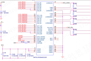
My customer use SN75LVDS84A and THC63LVDF84C as RGB to LVDS and LVDS to RGB bridge to screen.
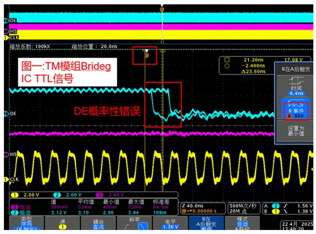
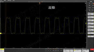
We meet a issue which is DE signal jitter , some time DE signal include more one clk. some time not.
They probe the THC63LVDF84C DE output. But they do the ABA test, we found the issue is follow the SN75LVDS84A.
So do you have some method to check if the LVDS output is correct?
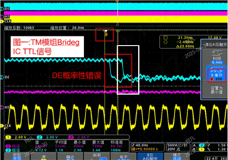
We also probe the DE signal input in SN75LVDS84A, which is good no jitter.
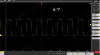
DE at SN75LVDS84A input.
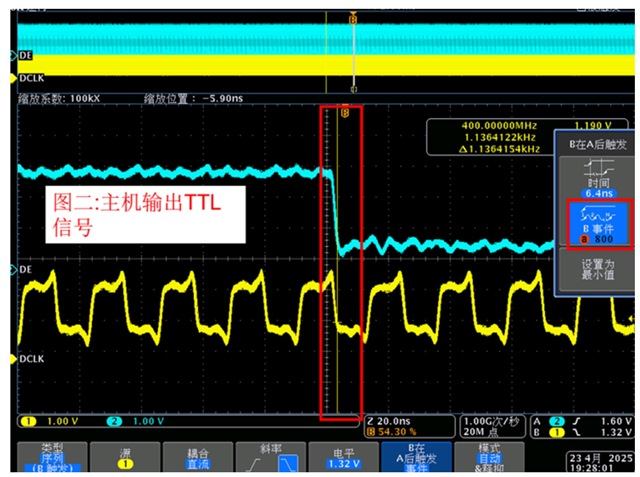
DE at THC63LVDF84C output: