Part Number: SN65DSI83
Other Parts Discussed in Thread: SN65DSI84
Tool/software:
Hi TI,
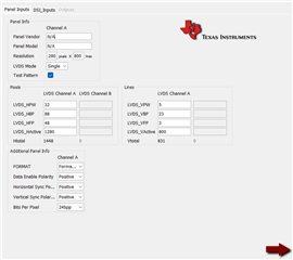
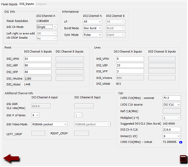
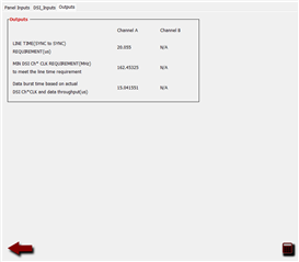
We are using a "RVT101HVDNWC00-B" which used "SN65DSI83" bridge, attached the block diagram and the data sheet for reference.
Below is the timing configuration which we have added:
static const struct drm_display_mode rvt101hvdnwc00_10 = {
    .clock = 71100,
    .hdisplay = 1280,
    .hsync_start = 1280 + 48,
    .hsync_end = 1280 + 48 + 32,
    .htotal = 1280 + 48 + 32 + 88,
    .vdisplay = 800,
    .vsync_start = 800 + 3,
    .vsync_end = 800 + 3 + 5,
    .vtotal = 800 + 3 + 5 + 22,
    .flags = DRM_MODE_FLAG_NHSYNC | DRM_MODE_FLAG_NVSYNC,
};

static const struct panel_desc rvt101hvdnwc00_10_10inch = {
    .modes = &rvt101hvdnwc00_10,
    .num_modes = 1,
    .bpc = 8,
    .size = {
        .width = 217,
        .height = 135,
    },
    .bus_format = MEDIA_BUS_FMT_RGB888_1X24,
    .connector_type = DRM_MODE_CONNECTOR_DSI,
};
It will be of great help if TI team could help us to generate the complete Register list based on the provided data,as we are unable to get the register list generated from the Tuner application.
Also we have attached the "SN65DSI83" Driver code in which we have commented the sn65dsi83_host_attach function as the device dosent use command line video configuration. Please verify the modification and let us know if the chnages are valid.
// SPDX-License-Identifier: GPL-2.0
/*
 * TI SN65DSI83,84,85 driver
 *
 * Currently supported:
 * - SN65DSI83
 *   = 1x Single-link DSI ~ 1x Single-link LVDS
 *   - Supported
 *   - Single-link LVDS mode tested
 * - SN65DSI84
 *   = 1x Single-link DSI ~ 2x Single-link or 1x Dual-link LVDS
 *   - Supported
 *   - Dual-link LVDS mode tested
 *   - 2x Single-link LVDS mode unsupported
 *     (should be easy to add by someone who has the HW)
 * - SN65DSI85
 *   = 2x Single-link or 1x Dual-link DSI ~ 2x Single-link or 1x Dual-link LVDS
 *   - Unsupported
 *     (should be easy to add by someone who has the HW)
 *
 * Copyright (C) 2021 Marek Vasut <marex@denx.de>
 *
 * Based on previous work of:
 * Valentin Raevsky <valentin@compulab.co.il>
 * Philippe Schenker <philippe.schenker@toradex.com>
 */

#include <linux/bits.h>
#include <linux/clk.h>
#include <linux/gpio/consumer.h>
#include <linux/i2c.h>
#include <linux/media-bus-format.h>
#include <linux/module.h>
#include <linux/of.h>
#include <linux/of_graph.h>
#include <linux/regmap.h>
#include <linux/regulator/consumer.h>

#include <drm/drm_atomic_helper.h>
#include <drm/drm_bridge.h>
#include <drm/drm_mipi_dsi.h>
#include <drm/drm_of.h>
#include <drm/drm_panel.h>
#include <drm/drm_print.h>
#include <drm/drm_probe_helper.h>

/* ID registers */
#define REG_ID(n)				(0x00 + (n))
/* Reset and clock registers */
#define REG_RC_RESET				0x09
#define  REG_RC_RESET_SOFT_RESET		BIT(0)
#define REG_RC_LVDS_PLL				0x0a
#define  REG_RC_LVDS_PLL_PLL_EN_STAT		BIT(7)
#define  REG_RC_LVDS_PLL_LVDS_CLK_RANGE(n)	(((n) & 0x7) << 1)
#define  REG_RC_LVDS_PLL_HS_CLK_SRC_DPHY	BIT(0)
#define REG_RC_DSI_CLK				0x0b
#define  REG_RC_DSI_CLK_DSI_CLK_DIVIDER(n)	(((n) & 0x1f) << 3)
#define  REG_RC_DSI_CLK_REFCLK_MULTIPLIER(n)	((n) & 0x3)
#define REG_RC_PLL_EN				0x0d
#define  REG_RC_PLL_EN_PLL_EN			BIT(0)
/* DSI registers */
#define REG_DSI_LANE				0x10
#define  REG_DSI_LANE_LEFT_RIGHT_PIXELS		BIT(7)	/* DSI85-only */
#define  REG_DSI_LANE_DSI_CHANNEL_MODE_DUAL	0	/* DSI85-only */
#define  REG_DSI_LANE_DSI_CHANNEL_MODE_2SINGLE	BIT(6)	/* DSI85-only */
#define  REG_DSI_LANE_DSI_CHANNEL_MODE_SINGLE	BIT(5)
#define  REG_DSI_LANE_CHA_DSI_LANES(n)		(((n) & 0x3) << 3)
#define  REG_DSI_LANE_CHB_DSI_LANES(n)		(((n) & 0x3) << 1)
#define  REG_DSI_LANE_SOT_ERR_TOL_DIS		BIT(0)
#define REG_DSI_EQ				0x11
#define  REG_DSI_EQ_CHA_DSI_DATA_EQ(n)		(((n) & 0x3) << 6)
#define  REG_DSI_EQ_CHA_DSI_CLK_EQ(n)		(((n) & 0x3) << 2)
#define REG_DSI_CLK				0x12
#define  REG_DSI_CLK_CHA_DSI_CLK_RANGE(n)	((n) & 0xff)
/* LVDS registers */
#define REG_LVDS_FMT				0x18
#define  REG_LVDS_FMT_DE_NEG_POLARITY		BIT(7)
#define  REG_LVDS_FMT_HS_NEG_POLARITY		BIT(6)
#define  REG_LVDS_FMT_VS_NEG_POLARITY		BIT(5)
#define  REG_LVDS_FMT_LVDS_LINK_CFG		BIT(4)	/* 0:AB 1:A-only */
#define  REG_LVDS_FMT_CHA_24BPP_MODE		BIT(3)
#define  REG_LVDS_FMT_CHB_24BPP_MODE		BIT(2)
#define  REG_LVDS_FMT_CHA_24BPP_FORMAT1		BIT(1)
#define  REG_LVDS_FMT_CHB_24BPP_FORMAT1		BIT(0)
#define REG_LVDS_VCOM				0x19
#define  REG_LVDS_VCOM_CHA_LVDS_VOCM		BIT(6)
#define  REG_LVDS_VCOM_CHB_LVDS_VOCM		BIT(4)
#define  REG_LVDS_VCOM_CHA_LVDS_VOD_SWING(n)	(((n) & 0x3) << 2)
#define  REG_LVDS_VCOM_CHB_LVDS_VOD_SWING(n)	((n) & 0x3)
#define REG_LVDS_LANE				0x1a
#define  REG_LVDS_LANE_EVEN_ODD_SWAP		BIT(6)
#define  REG_LVDS_LANE_CHA_REVERSE_LVDS		BIT(5)
#define  REG_LVDS_LANE_CHB_REVERSE_LVDS		BIT(4)
#define  REG_LVDS_LANE_CHA_LVDS_TERM		BIT(1)
#define  REG_LVDS_LANE_CHB_LVDS_TERM		BIT(0)
#define REG_LVDS_CM				0x1b
#define  REG_LVDS_CM_CHA_LVDS_CM_ADJUST(n)	(((n) & 0x3) << 4)
#define  REG_LVDS_CM_CHB_LVDS_CM_ADJUST(n)	((n) & 0x3)
/* Video registers */
#define REG_VID_CHA_ACTIVE_LINE_LENGTH_LOW	0x20
#define REG_VID_CHA_ACTIVE_LINE_LENGTH_HIGH	0x21
#define REG_VID_CHA_VERTICAL_DISPLAY_SIZE_LOW	0x24
#define REG_VID_CHA_VERTICAL_DISPLAY_SIZE_HIGH	0x25
#define REG_VID_CHA_SYNC_DELAY_LOW		0x28
#define REG_VID_CHA_SYNC_DELAY_HIGH		0x29
#define REG_VID_CHA_HSYNC_PULSE_WIDTH_LOW	0x2c
#define REG_VID_CHA_HSYNC_PULSE_WIDTH_HIGH	0x2d
#define REG_VID_CHA_VSYNC_PULSE_WIDTH_LOW	0x30
#define REG_VID_CHA_VSYNC_PULSE_WIDTH_HIGH	0x31
#define REG_VID_CHA_HORIZONTAL_BACK_PORCH	0x34
#define REG_VID_CHA_VERTICAL_BACK_PORCH		0x36
#define REG_VID_CHA_HORIZONTAL_FRONT_PORCH	0x38
#define REG_VID_CHA_VERTICAL_FRONT_PORCH	0x3a
#define REG_VID_CHA_TEST_PATTERN		0x3c
/* IRQ registers */
#define REG_IRQ_GLOBAL				0xe0
#define  REG_IRQ_GLOBAL_IRQ_EN			BIT(0)
#define REG_IRQ_EN				0xe1
#define  REG_IRQ_EN_CHA_SYNCH_ERR_EN		BIT(7)
#define  REG_IRQ_EN_CHA_CRC_ERR_EN		BIT(6)
#define  REG_IRQ_EN_CHA_UNC_ECC_ERR_EN		BIT(5)
#define  REG_IRQ_EN_CHA_COR_ECC_ERR_EN		BIT(4)
#define  REG_IRQ_EN_CHA_LLP_ERR_EN		BIT(3)
#define  REG_IRQ_EN_CHA_SOT_BIT_ERR_EN		BIT(2)
#define  REG_IRQ_EN_CHA_PLL_UNLOCK_EN		BIT(0)
#define REG_IRQ_STAT				0xe5
#define  REG_IRQ_STAT_CHA_SYNCH_ERR		BIT(7)
#define  REG_IRQ_STAT_CHA_CRC_ERR		BIT(6)
#define  REG_IRQ_STAT_CHA_UNC_ECC_ERR		BIT(5)
#define  REG_IRQ_STAT_CHA_COR_ECC_ERR		BIT(4)
#define  REG_IRQ_STAT_CHA_LLP_ERR		BIT(3)
#define  REG_IRQ_STAT_CHA_SOT_BIT_ERR		BIT(2)
#define  REG_IRQ_STAT_CHA_PLL_UNLOCK		BIT(0)

enum sn65dsi83_model {
	MODEL_SN65DSI83,
	MODEL_SN65DSI84,
};

struct sn65dsi83 {
	struct drm_bridge		bridge;
	struct device			*dev;
	struct regmap			*regmap;
	struct mipi_dsi_device		*dsi;
	struct drm_bridge		*panel_bridge;
	struct gpio_desc		*enable_gpio;
	struct regulator		*vcc;
	bool				lvds_dual_link;
	bool				lvds_dual_link_even_odd_swap;
};

static const struct regmap_range sn65dsi83_readable_ranges[] = {
	regmap_reg_range(REG_ID(0), REG_ID(8)),
	regmap_reg_range(REG_RC_LVDS_PLL, REG_RC_DSI_CLK),
	regmap_reg_range(REG_RC_PLL_EN, REG_RC_PLL_EN),
	regmap_reg_range(REG_DSI_LANE, REG_DSI_CLK),
	regmap_reg_range(REG_LVDS_FMT, REG_LVDS_CM),
	regmap_reg_range(REG_VID_CHA_ACTIVE_LINE_LENGTH_LOW,
			 REG_VID_CHA_ACTIVE_LINE_LENGTH_HIGH),
	regmap_reg_range(REG_VID_CHA_VERTICAL_DISPLAY_SIZE_LOW,
			 REG_VID_CHA_VERTICAL_DISPLAY_SIZE_HIGH),
	regmap_reg_range(REG_VID_CHA_SYNC_DELAY_LOW,
			 REG_VID_CHA_SYNC_DELAY_HIGH),
	regmap_reg_range(REG_VID_CHA_HSYNC_PULSE_WIDTH_LOW,
			 REG_VID_CHA_HSYNC_PULSE_WIDTH_HIGH),
	regmap_reg_range(REG_VID_CHA_VSYNC_PULSE_WIDTH_LOW,
			 REG_VID_CHA_VSYNC_PULSE_WIDTH_HIGH),
	regmap_reg_range(REG_VID_CHA_HORIZONTAL_BACK_PORCH,
			 REG_VID_CHA_HORIZONTAL_BACK_PORCH),
	regmap_reg_range(REG_VID_CHA_VERTICAL_BACK_PORCH,
			 REG_VID_CHA_VERTICAL_BACK_PORCH),
	regmap_reg_range(REG_VID_CHA_HORIZONTAL_FRONT_PORCH,
			 REG_VID_CHA_HORIZONTAL_FRONT_PORCH),
	regmap_reg_range(REG_VID_CHA_VERTICAL_FRONT_PORCH,
			 REG_VID_CHA_VERTICAL_FRONT_PORCH),
	regmap_reg_range(REG_VID_CHA_TEST_PATTERN, REG_VID_CHA_TEST_PATTERN),
	regmap_reg_range(REG_IRQ_GLOBAL, REG_IRQ_EN),
	regmap_reg_range(REG_IRQ_STAT, REG_IRQ_STAT),
};

static const struct regmap_access_table sn65dsi83_readable_table = {
	.yes_ranges = sn65dsi83_readable_ranges,
	.n_yes_ranges = ARRAY_SIZE(sn65dsi83_readable_ranges),
};

static const struct regmap_range sn65dsi83_writeable_ranges[] = {
	regmap_reg_range(REG_RC_RESET, REG_RC_DSI_CLK),
	regmap_reg_range(REG_RC_PLL_EN, REG_RC_PLL_EN),
	regmap_reg_range(REG_DSI_LANE, REG_DSI_CLK),
	regmap_reg_range(REG_LVDS_FMT, REG_LVDS_CM),
	regmap_reg_range(REG_VID_CHA_ACTIVE_LINE_LENGTH_LOW,
			 REG_VID_CHA_ACTIVE_LINE_LENGTH_HIGH),
	regmap_reg_range(REG_VID_CHA_VERTICAL_DISPLAY_SIZE_LOW,
			 REG_VID_CHA_VERTICAL_DISPLAY_SIZE_HIGH),
	regmap_reg_range(REG_VID_CHA_SYNC_DELAY_LOW,
			 REG_VID_CHA_SYNC_DELAY_HIGH),
	regmap_reg_range(REG_VID_CHA_HSYNC_PULSE_WIDTH_LOW,
			 REG_VID_CHA_HSYNC_PULSE_WIDTH_HIGH),
	regmap_reg_range(REG_VID_CHA_VSYNC_PULSE_WIDTH_LOW,
			 REG_VID_CHA_VSYNC_PULSE_WIDTH_HIGH),
	regmap_reg_range(REG_VID_CHA_HORIZONTAL_BACK_PORCH,
			 REG_VID_CHA_HORIZONTAL_BACK_PORCH),
	regmap_reg_range(REG_VID_CHA_VERTICAL_BACK_PORCH,
			 REG_VID_CHA_VERTICAL_BACK_PORCH),
	regmap_reg_range(REG_VID_CHA_HORIZONTAL_FRONT_PORCH,
			 REG_VID_CHA_HORIZONTAL_FRONT_PORCH),
	regmap_reg_range(REG_VID_CHA_VERTICAL_FRONT_PORCH,
			 REG_VID_CHA_VERTICAL_FRONT_PORCH),
	regmap_reg_range(REG_VID_CHA_TEST_PATTERN, REG_VID_CHA_TEST_PATTERN),
	regmap_reg_range(REG_IRQ_GLOBAL, REG_IRQ_EN),
	regmap_reg_range(REG_IRQ_STAT, REG_IRQ_STAT),
};

static const struct regmap_access_table sn65dsi83_writeable_table = {
	.yes_ranges = sn65dsi83_writeable_ranges,
	.n_yes_ranges = ARRAY_SIZE(sn65dsi83_writeable_ranges),
};

static const struct regmap_range sn65dsi83_volatile_ranges[] = {
	regmap_reg_range(REG_RC_RESET, REG_RC_RESET),
	regmap_reg_range(REG_RC_LVDS_PLL, REG_RC_LVDS_PLL),
	regmap_reg_range(REG_IRQ_STAT, REG_IRQ_STAT),
};

static const struct regmap_access_table sn65dsi83_volatile_table = {
	.yes_ranges = sn65dsi83_volatile_ranges,
	.n_yes_ranges = ARRAY_SIZE(sn65dsi83_volatile_ranges),
};

static const struct regmap_config sn65dsi83_regmap_config = {
	.reg_bits = 8,
	.val_bits = 8,
	.rd_table = &sn65dsi83_readable_table,
	.wr_table = &sn65dsi83_writeable_table,
	.volatile_table = &sn65dsi83_volatile_table,
	.cache_type = REGCACHE_RBTREE,
	.max_register = REG_IRQ_STAT,
};

static struct sn65dsi83 *bridge_to_sn65dsi83(struct drm_bridge *bridge)
{
	return container_of(bridge, struct sn65dsi83, bridge);
}

static int sn65dsi83_attach(struct drm_bridge *bridge,
			    enum drm_bridge_attach_flags flags)
{
	struct sn65dsi83 *ctx = bridge_to_sn65dsi83(bridge);

	return drm_bridge_attach(bridge->encoder, ctx->panel_bridge,
				 &ctx->bridge, flags);
}

static void sn65dsi83_detach(struct drm_bridge *bridge)
{
	struct sn65dsi83 *ctx = bridge_to_sn65dsi83(bridge);

	if (!ctx->dsi)
		return;

	ctx->dsi = NULL;
}

static u8 sn65dsi83_get_lvds_range(struct sn65dsi83 *ctx,
				   const struct drm_display_mode *mode)
{
	/*
	 * The encoding of the LVDS_CLK_RANGE is as follows:
	 * 000 - 25 MHz <= LVDS_CLK < 37.5 MHz
	 * 001 - 37.5 MHz <= LVDS_CLK < 62.5 MHz
	 * 010 - 62.5 MHz <= LVDS_CLK < 87.5 MHz
	 * 011 - 87.5 MHz <= LVDS_CLK < 112.5 MHz
	 * 100 - 112.5 MHz <= LVDS_CLK < 137.5 MHz
	 * 101 - 137.5 MHz <= LVDS_CLK <= 154 MHz
	 * which is a range of 12.5MHz..162.5MHz in 50MHz steps, except that
	 * the ends of the ranges are clamped to the supported range. Since
	 * sn65dsi83_mode_valid() already filters the valid modes and limits
	 * the clock to 25..154 MHz, the range calculation can be simplified
	 * as follows:
	 */
	int mode_clock = mode->clock;

	if (ctx->lvds_dual_link)
		mode_clock /= 2;

	return (mode_clock - 12500) / 25000;
}

static u8 sn65dsi83_get_dsi_range(struct sn65dsi83 *ctx,
				  const struct drm_display_mode *mode)
{
	/*
	 * The encoding of the CHA_DSI_CLK_RANGE is as follows:
	 * 0x00 through 0x07 - Reserved
	 * 0x08 - 40 <= DSI_CLK < 45 MHz
	 * 0x09 - 45 <= DSI_CLK < 50 MHz
	 * ...
	 * 0x63 - 495 <= DSI_CLK < 500 MHz
	 * 0x64 - 500 MHz
	 * 0x65 through 0xFF - Reserved
	 * which is DSI clock in 5 MHz steps, clamped to 40..500 MHz.
	 * The DSI clock are calculated as:
	 *  DSI_CLK = mode clock * bpp / dsi_data_lanes / 2
	 * the 2 is there because the bus is DDR.
	 */
	return DIV_ROUND_UP(clamp((unsigned int)mode->clock *
			    mipi_dsi_pixel_format_to_bpp(ctx->dsi->format) /
			    ctx->dsi->lanes / 2, 40000U, 500000U), 5000U);
}

static u8 sn65dsi83_get_dsi_div(struct sn65dsi83 *ctx)
{
	/* The divider is (DSI_CLK / LVDS_CLK) - 1, which really is: */
	unsigned int dsi_div = mipi_dsi_pixel_format_to_bpp(ctx->dsi->format);

	dsi_div /= ctx->dsi->lanes;

	if (!ctx->lvds_dual_link)
		dsi_div /= 2;

	return dsi_div - 1;
}

static void sn65dsi83_atomic_pre_enable(struct drm_bridge *bridge,
					struct drm_bridge_state *old_bridge_state)
{
	struct sn65dsi83 *ctx = bridge_to_sn65dsi83(bridge);
	struct drm_atomic_state *state = old_bridge_state->base.state;
	const struct drm_bridge_state *bridge_state;
	const struct drm_crtc_state *crtc_state;
	const struct drm_display_mode *mode;
	struct drm_connector *connector;
	struct drm_crtc *crtc;
	bool lvds_format_24bpp;
	bool lvds_format_jeida;
	unsigned int pval;
	__le16 le16val;
	u16 val;
	int ret;

	ret = regulator_enable(ctx->vcc);
	if (ret) {
		dev_err(ctx->dev, "Failed to enable vcc: %d\n", ret);
		return;
	}

	/* Deassert reset */
	gpiod_set_value_cansleep(ctx->enable_gpio, 1);
	usleep_range(10000, 11000);

	/* Get the LVDS format from the bridge state. */
	bridge_state = drm_atomic_get_new_bridge_state(state, bridge);

	switch (bridge_state->output_bus_cfg.format) {
	case MEDIA_BUS_FMT_RGB666_1X7X3_SPWG:
		lvds_format_24bpp = false;
		lvds_format_jeida = true;
		break;
	case MEDIA_BUS_FMT_RGB888_1X7X4_JEIDA:
		lvds_format_24bpp = true;
		lvds_format_jeida = true;
		break;
	case MEDIA_BUS_FMT_RGB888_1X7X4_SPWG:
		lvds_format_24bpp = true;
		lvds_format_jeida = false;
		break;
	default:
		/*
		 * Some bridges still don't set the correct
		 * LVDS bus pixel format, use SPWG24 default
		 * format until those are fixed.
		 */
		lvds_format_24bpp = true;
		lvds_format_jeida = false;
		dev_warn(ctx->dev,
			 "Unsupported LVDS bus format 0x%04x, please check output bridge driver. Falling back to SPWG24.\n",
			 bridge_state->output_bus_cfg.format);
		break;
	}

	/*
	 * Retrieve the CRTC adjusted mode. This requires a little dance to go
	 * from the bridge to the encoder, to the connector and to the CRTC.
	 */
	connector = drm_atomic_get_new_connector_for_encoder(state,
							     bridge->encoder);
	crtc = drm_atomic_get_new_connector_state(state, connector)->crtc;
	crtc_state = drm_atomic_get_new_crtc_state(state, crtc);
	mode = &crtc_state->adjusted_mode;

	/* Clear reset, disable PLL */
	regmap_write(ctx->regmap, REG_RC_RESET, 0x00);
	regmap_write(ctx->regmap, REG_RC_PLL_EN, 0x00);

	/* Reference clock derived from DSI link clock. */
	regmap_write(ctx->regmap, REG_RC_LVDS_PLL,
		     REG_RC_LVDS_PLL_LVDS_CLK_RANGE(sn65dsi83_get_lvds_range(ctx, mode)) |
		     REG_RC_LVDS_PLL_HS_CLK_SRC_DPHY);
	regmap_write(ctx->regmap, REG_DSI_CLK,
		     REG_DSI_CLK_CHA_DSI_CLK_RANGE(sn65dsi83_get_dsi_range(ctx, mode)));
	regmap_write(ctx->regmap, REG_RC_DSI_CLK,
		     REG_RC_DSI_CLK_DSI_CLK_DIVIDER(sn65dsi83_get_dsi_div(ctx)));

	/* Set number of DSI lanes and LVDS link config. */
	regmap_write(ctx->regmap, REG_DSI_LANE,
		     REG_DSI_LANE_DSI_CHANNEL_MODE_SINGLE |
		     REG_DSI_LANE_CHA_DSI_LANES(~(ctx->dsi->lanes - 1)) |
		     /* CHB is DSI85-only, set to default on DSI83/DSI84 */
		     REG_DSI_LANE_CHB_DSI_LANES(3));
	/* No equalization. */
	regmap_write(ctx->regmap, REG_DSI_EQ, 0x00);

	/* Set up sync signal polarity. */
	val = (mode->flags & DRM_MODE_FLAG_NHSYNC ?
	       REG_LVDS_FMT_HS_NEG_POLARITY : 0) |
	      (mode->flags & DRM_MODE_FLAG_NVSYNC ?
	       REG_LVDS_FMT_VS_NEG_POLARITY : 0);

	/* Set up bits-per-pixel, 18bpp or 24bpp. */
	if (lvds_format_24bpp) {
		val |= REG_LVDS_FMT_CHA_24BPP_MODE;
		if (ctx->lvds_dual_link)
			val |= REG_LVDS_FMT_CHB_24BPP_MODE;
	}

	/* Set up LVDS format, JEIDA/Format 1 or SPWG/Format 2 */
	if (lvds_format_jeida) {
		val |= REG_LVDS_FMT_CHA_24BPP_FORMAT1;
		if (ctx->lvds_dual_link)
			val |= REG_LVDS_FMT_CHB_24BPP_FORMAT1;
	}

	/* Set up LVDS output config (DSI84,DSI85) */
	if (!ctx->lvds_dual_link)
		val |= REG_LVDS_FMT_LVDS_LINK_CFG;

	regmap_write(ctx->regmap, REG_LVDS_FMT, val);
	regmap_write(ctx->regmap, REG_LVDS_VCOM, 0x05);
	regmap_write(ctx->regmap, REG_LVDS_LANE,
		     (ctx->lvds_dual_link_even_odd_swap ?
		      REG_LVDS_LANE_EVEN_ODD_SWAP : 0) |
		     REG_LVDS_LANE_CHA_LVDS_TERM |
		     REG_LVDS_LANE_CHB_LVDS_TERM);
	regmap_write(ctx->regmap, REG_LVDS_CM, 0x00);

	le16val = cpu_to_le16(mode->hdisplay);
	regmap_bulk_write(ctx->regmap, REG_VID_CHA_ACTIVE_LINE_LENGTH_LOW,
			  &le16val, 2);
	le16val = cpu_to_le16(mode->vdisplay);
	regmap_bulk_write(ctx->regmap, REG_VID_CHA_VERTICAL_DISPLAY_SIZE_LOW,
			  &le16val, 2);
	/* 32 + 1 pixel clock to ensure proper operation */
	le16val = cpu_to_le16(32 + 1);
	regmap_bulk_write(ctx->regmap, REG_VID_CHA_SYNC_DELAY_LOW, &le16val, 2);
	le16val = cpu_to_le16(mode->hsync_end - mode->hsync_start);
	regmap_bulk_write(ctx->regmap, REG_VID_CHA_HSYNC_PULSE_WIDTH_LOW,
			  &le16val, 2);
	le16val = cpu_to_le16(mode->vsync_end - mode->vsync_start);
	regmap_bulk_write(ctx->regmap, REG_VID_CHA_VSYNC_PULSE_WIDTH_LOW,
			  &le16val, 2);
	regmap_write(ctx->regmap, REG_VID_CHA_HORIZONTAL_BACK_PORCH,
		     mode->htotal - mode->hsync_end);
	regmap_write(ctx->regmap, REG_VID_CHA_VERTICAL_BACK_PORCH,
		     mode->vtotal - mode->vsync_end);
	regmap_write(ctx->regmap, REG_VID_CHA_HORIZONTAL_FRONT_PORCH,
		     mode->hsync_start - mode->hdisplay);
	regmap_write(ctx->regmap, REG_VID_CHA_VERTICAL_FRONT_PORCH,
		     mode->vsync_start - mode->vdisplay);
	regmap_write(ctx->regmap, REG_VID_CHA_TEST_PATTERN, 0x00);

	/* Enable PLL */
	regmap_write(ctx->regmap, REG_RC_PLL_EN, REG_RC_PLL_EN_PLL_EN);
	usleep_range(3000, 4000);
	ret = regmap_read_poll_timeout(ctx->regmap, REG_RC_LVDS_PLL, pval,
				       pval & REG_RC_LVDS_PLL_PLL_EN_STAT,
				       1000, 100000);
	if (ret) {
		dev_err(ctx->dev, "failed to lock PLL, ret=%i\n", ret);
		/* On failure, disable PLL again and exit. */
		regmap_write(ctx->regmap, REG_RC_PLL_EN, 0x00);
		regulator_disable(ctx->vcc);
		return;
	}

	/* Trigger reset after CSR register update. */
	regmap_write(ctx->regmap, REG_RC_RESET, REG_RC_RESET_SOFT_RESET);

	/* Wait for 10ms after soft reset as specified in datasheet */
	usleep_range(10000, 12000);
}

static void sn65dsi83_atomic_enable(struct drm_bridge *bridge,
				    struct drm_bridge_state *old_bridge_state)
{
	struct sn65dsi83 *ctx = bridge_to_sn65dsi83(bridge);
	unsigned int pval;

	/* Clear all errors that got asserted during initialization. */
	regmap_read(ctx->regmap, REG_IRQ_STAT, &pval);
	regmap_write(ctx->regmap, REG_IRQ_STAT, pval);

	/* Wait for 1ms and check for errors in status register */
	usleep_range(1000, 1100);
	regmap_read(ctx->regmap, REG_IRQ_STAT, &pval);
	if (pval)
		dev_err(ctx->dev, "Unexpected link status 0x%02x\n", pval);
}

static void sn65dsi83_atomic_disable(struct drm_bridge *bridge,
				     struct drm_bridge_state *old_bridge_state)
{
	struct sn65dsi83 *ctx = bridge_to_sn65dsi83(bridge);
	int ret;

	/* Put the chip in reset, pull EN line low, and assure 10ms reset low timing. */
	gpiod_set_value_cansleep(ctx->enable_gpio, 0);
	usleep_range(10000, 11000);

	ret = regulator_disable(ctx->vcc);
	if (ret)
		dev_err(ctx->dev, "Failed to disable vcc: %d\n", ret);

	regcache_mark_dirty(ctx->regmap);
}

static enum drm_mode_status
sn65dsi83_mode_valid(struct drm_bridge *bridge,
		     const struct drm_display_info *info,
		     const struct drm_display_mode *mode)
{
	/* LVDS output clock range 25..154 MHz */
	if (mode->clock < 25000)
		return MODE_CLOCK_LOW;
	if (mode->clock > 154000)
		return MODE_CLOCK_HIGH;

	return MODE_OK;
}

#define MAX_INPUT_SEL_FORMATS	1

static u32 *
sn65dsi83_atomic_get_input_bus_fmts(struct drm_bridge *bridge,
				    struct drm_bridge_state *bridge_state,
				    struct drm_crtc_state *crtc_state,
				    struct drm_connector_state *conn_state,
				    u32 output_fmt,
				    unsigned int *num_input_fmts)
{
	u32 *input_fmts;

	*num_input_fmts = 0;

	input_fmts = kcalloc(MAX_INPUT_SEL_FORMATS, sizeof(*input_fmts),
			     GFP_KERNEL);
	if (!input_fmts)
		return NULL;

	/* This is the DSI-end bus format */
	input_fmts[0] = MEDIA_BUS_FMT_RGB888_1X24;
	*num_input_fmts = 1;

	return input_fmts;
}

static const struct drm_bridge_funcs sn65dsi83_funcs = {
	.attach			= sn65dsi83_attach,
	.detach			= sn65dsi83_detach,
	.atomic_enable		= sn65dsi83_atomic_enable,
	.atomic_pre_enable	= sn65dsi83_atomic_pre_enable,
	.atomic_disable		= sn65dsi83_atomic_disable,
	.mode_valid		= sn65dsi83_mode_valid,

	.atomic_duplicate_state = drm_atomic_helper_bridge_duplicate_state,
	.atomic_destroy_state = drm_atomic_helper_bridge_destroy_state,
	.atomic_reset = drm_atomic_helper_bridge_reset,
	.atomic_get_input_bus_fmts = sn65dsi83_atomic_get_input_bus_fmts,
};

static int sn65dsi83_parse_dt(struct sn65dsi83 *ctx, enum sn65dsi83_model model)
{
	struct drm_bridge *panel_bridge;
	struct device *dev = ctx->dev;

	ctx->lvds_dual_link = false;
	ctx->lvds_dual_link_even_odd_swap = false;
	if (model != MODEL_SN65DSI83) {
		struct device_node *port2, *port3;
		int dual_link;

		port2 = of_graph_get_port_by_id(dev->of_node, 2);
		port3 = of_graph_get_port_by_id(dev->of_node, 3);
		dual_link = drm_of_lvds_get_dual_link_pixel_order(port2, port3);
		of_node_put(port2);
		of_node_put(port3);

		if (dual_link == DRM_LVDS_DUAL_LINK_ODD_EVEN_PIXELS) {
			ctx->lvds_dual_link = true;
			/* Odd pixels to LVDS Channel A, even pixels to B */
			ctx->lvds_dual_link_even_odd_swap = false;
		} else if (dual_link == DRM_LVDS_DUAL_LINK_EVEN_ODD_PIXELS) {
			ctx->lvds_dual_link = true;
			/* Even pixels to LVDS Channel A, odd pixels to B */
			ctx->lvds_dual_link_even_odd_swap = true;
		}
	}

	panel_bridge = devm_drm_of_get_bridge(dev, dev->of_node, 2, 0);
	if (IS_ERR(panel_bridge))
		return PTR_ERR(panel_bridge);

	ctx->panel_bridge = panel_bridge;

	ctx->vcc = devm_regulator_get(dev, "vcc");
	if (IS_ERR(ctx->vcc))
		return dev_err_probe(dev, PTR_ERR(ctx->vcc),
				     "Failed to get supply 'vcc'\n");

	return 0;
}

static int sn65dsi83_host_attach(struct sn65dsi83 *ctx)
{
	struct device *dev = ctx->dev;
	struct device_node *host_node;
	struct device_node *endpoint;
	struct mipi_dsi_device *dsi;
	struct mipi_dsi_host *host;
	const struct mipi_dsi_device_info info = {
		.type = "sn65dsi83",
		.channel = 0,
		.node = NULL,
	};
	int dsi_lanes, ret;

	endpoint = of_graph_get_endpoint_by_regs(dev->of_node, 0, -1);
	dsi_lanes = drm_of_get_data_lanes_count(endpoint, 1, 4);
	host_node = of_graph_get_remote_port_parent(endpoint);
	host = of_find_mipi_dsi_host_by_node(host_node);
	of_node_put(host_node);
	of_node_put(endpoint);

	if (!host)
		return -EPROBE_DEFER;

	if (dsi_lanes < 0)
		return dsi_lanes;

	dsi = devm_mipi_dsi_device_register_full(dev, host, &info);
	if (IS_ERR(dsi))
		return dev_err_probe(dev, PTR_ERR(dsi),
				     "failed to create dsi device\n");

	ctx->dsi = dsi;

	dsi->lanes = dsi_lanes;
	dsi->format = MIPI_DSI_FMT_RGB888;
	dsi->mode_flags = MIPI_DSI_MODE_VIDEO | MIPI_DSI_MODE_VIDEO_BURST |
			  MIPI_DSI_MODE_VIDEO_NO_HFP | MIPI_DSI_MODE_VIDEO_NO_HBP |
			  MIPI_DSI_MODE_VIDEO_NO_HSA | MIPI_DSI_MODE_NO_EOT_PACKET;

	ret = devm_mipi_dsi_attach(dev, dsi);
	if (ret < 0) {
		dev_err(dev, "failed to attach dsi to host: %d\n", ret);
		return ret;
	}

	return 0;
}

static int sn65dsi83_probe(struct i2c_client *client)
{
	const struct i2c_device_id *id = i2c_client_get_device_id(client);
	struct device *dev = &client->dev;
	enum sn65dsi83_model model;
	struct sn65dsi83 *ctx;
	int ret;

	printk("Zumi %s %d \r\n", __func__, __LINE__);
	ctx = devm_kzalloc(dev, sizeof(*ctx), GFP_KERNEL);
	if (!ctx)
		return -ENOMEM;

	ctx->dev = dev;

	if (dev->of_node) {
		model = (enum sn65dsi83_model)(uintptr_t)
			of_device_get_match_data(dev);
	} else {
		model = id->driver_data;
	}

	/* Put the chip in reset, pull EN line low, and assure 10ms reset low timing. */
	ctx->enable_gpio = devm_gpiod_get_optional(ctx->dev, "enable",
						   GPIOD_OUT_LOW);
	if (IS_ERR(ctx->enable_gpio))
		return dev_err_probe(dev, PTR_ERR(ctx->enable_gpio), "failed to get enable GPIO\n");

	usleep_range(10000, 11000);

	ret = sn65dsi83_parse_dt(ctx, model);
	if (ret)
		return ret;

	ctx->regmap = devm_regmap_init_i2c(client, &sn65dsi83_regmap_config);
	if (IS_ERR(ctx->regmap))
		return dev_err_probe(dev, PTR_ERR(ctx->regmap), "failed to get regmap\n");

	dev_set_drvdata(dev, ctx);
	i2c_set_clientdata(client, ctx);

	ctx->bridge.funcs = &sn65dsi83_funcs;
	ctx->bridge.of_node = dev->of_node;
	ctx->bridge.pre_enable_prev_first = true;
	drm_bridge_add(&ctx->bridge);
#if 0
	ret = sn65dsi83_host_attach(ctx);
	if (ret) {
		dev_err_probe(dev, ret, "failed to attach DSI host\n");
		goto err_remove_bridge;
	}
#endif
	return 0;
#if 0
err_remove_bridge:
	drm_bridge_remove(&ctx->bridge);
	return ret;
#endif
}

static void sn65dsi83_remove(struct i2c_client *client)
{
	struct sn65dsi83 *ctx = i2c_get_clientdata(client);

	drm_bridge_remove(&ctx->bridge);
}

static struct i2c_device_id sn65dsi83_id[] = {
	{ "ti,sn65dsi83", MODEL_SN65DSI83 },
	{ "ti,sn65dsi84", MODEL_SN65DSI84 },
	{},
};
MODULE_DEVICE_TABLE(i2c, sn65dsi83_id);

static const struct of_device_id sn65dsi83_match_table[] = {
	{ .compatible = "ti,sn65dsi83", .data = (void *)MODEL_SN65DSI83 },
	{ .compatible = "ti,sn65dsi84", .data = (void *)MODEL_SN65DSI84 },
	{},
};
MODULE_DEVICE_TABLE(of, sn65dsi83_match_table);

static struct i2c_driver sn65dsi83_driver = {
	.probe = sn65dsi83_probe,
	.remove = sn65dsi83_remove,
	.id_table = sn65dsi83_id,
	.driver = {
		.name = "sn65dsi83",
		.of_match_table = sn65dsi83_match_table,
	},
};
module_i2c_driver(sn65dsi83_driver);

MODULE_AUTHOR("Marek Vasut <marex@denx.de>");
MODULE_DESCRIPTION("TI SN65DSI83 DSI to LVDS bridge driver");
MODULE_LICENSE("GPL v2");
Note: With this changes we are able to get card0 and card0-LVDS-1 nodes in /sys/class/drm. Also attached the modetest logs for reference
root@imx93Oraclemain:~# modetest -M imx-drm
Encoders:
id      crtc    type    possible crtcs  possible clones
34      0       DSI     0x00000001      0x00000001

Connectors:
id      encoder status          name            size (mm)       modes   encoders
35      0       connected       LVDS-1          217x135         0       34
  props:
        1 EDID:
                flags: immutable blob
                blobs:

                value:
        2 DPMS:
                flags: enum
                enums: On=0 Standby=1 Suspend=2 Off=3
                value: 0
        5 link-status:
                flags: enum
                enums: Good=0 Bad=1
                value: 0
        6 non-desktop:
                flags: immutable range
                values: 0 1
                value: 0
        4 TILE:
                flags: immutable blob
                blobs:

                value:

CRTCs:
id      fb      pos     size
33      0       (0,0)   (0x0)
  #0  nan 0 0 0 0 0 0 0 0 0 flags: ; type:
  props:
        24 VRR_ENABLED:
                flags: range
                values: 0 1
                value: 0

Planes:
id      crtc    fb      CRTC x,y        x,y     gamma size      possible crtcs
31      0       0       0,0             0,0     0               0x00000001
  formats: XR24 AR24 RG16 XB24 AB24 AR15 XR15
  props:
        8 type:
                flags: immutable enum
                enums: Overlay=0 Primary=1 Cursor=2
                value: 1
        32 zpos:
                flags: immutable range
                values: 0 0
                value: 0

Frame buffers:
id      size    pitch