Tool/software:
Hi TIer
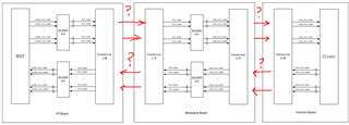
Where is the DS160PR410 recommended on the PCIE link?
Are they near the transmitter, near the receiver, near the board connector end, or are they not explicitly required?
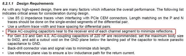
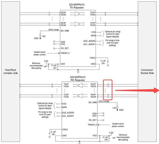
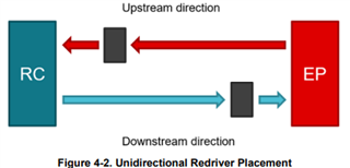
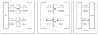
Our current layout design is to place the two DS160PR410 on the TX and RX links near the COME of the PC board and two more at the backplane near the connector, as shown in the box below, note the relative position of the capacitance. May I know if it is possible to put only one DS160PR410 at the transmission end, without the DS160PR410 reserved for the backplane? Or just place two DS160PR410 on the back panel, not on the PC board?