This thread has been locked.

If you have a related question, please click the "Ask a related question" button in the top right corner. The newly created question will be automatically linked to this question.

AM26C31: Could TI provide the output impedance details for both old (AM26C31ID, AM26C31IDG4, AM26C31IDRG4) and new die part (AM26C31IDR) ?

Part Number: AM26C31

Tool/software:

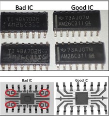
Factory has encountered a high fallout at production after supplier cut in the new die (see x-ray) chip.

So please answer to the highlighted Bold questions in the below summary.


Pin

Pin Description

Remark

7

GP_SYNC

Test verify signal is 3.95V±1.55V; pulse width 1.028 ±1%

9

GP_DATA_TX

Test verify DATA transmit out and receive.

10

GP_OUT+

Test verify signal is 125kHz ±10%; with 50% ± duty cycle; with amplitude 3.95V±1.55V

15

GP_CLK

Test verify signal is 250kHz ±10%; with 50% ± duty cycle; with amplitude 3.95V±1.55V


U14 (AM26C31I) on the board convert single ended signal GP_DATA_TX to positive differential signal (GP_OUT+, pin 10) and negative differential signal (GP_OUT-, pin 11).

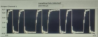
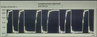
  • A sub-test is executed to measure the differential DATA (125kHz), duty cycle (50%) and amplitude (2.4-5.5V) for GP_OUT+ signal. See modular oscilloscope signal captured by tester.  
  • Failures are mainly related to clock (~260kHz) and duty cycle (97.7%).     
  • Each of the differential output has a series resistance 40 ohms. The sub-test pass when the series resistor value reduced (33 ohms – 36 ohms). There is an indication of the new die AM26C31IDR differential output impedance had changed but PCN claimed no form, fit and function affected. The failed board is reworked with old die (with suffix G4) and it able to pass the sub-test. Could TI provide the output impedance for both old (AM26C31ID, AM26C31IDG4, AM26C31IDRG4) and new die part (AM26C31IDR) ?  

  • The lead frame (example pin 1,2,7,8,9,10,15,16), internal team has a question whether the out impedance is still identical between the old part and new part?


  • Also need your support to know what’s the date code and assembly site for these 2 parts AM26C311LDRG4 and AM26C31LDR.

    Help us to guide how we can get this information from your TI site for future reference.

    So, it helps us to conclude was it impacted after this PCN implementation: 20240328001.1

  • When the PCN says that the function has not changed, it means that all guaranteed datasheet parameters stay the same. The datasheet guarantees that with a 100 Ω load, the differential output voltage is at least 2 V.

    Anyway, how does your test measure the duty cycle? In the captured waveforms, the duty cycle looks OK. Do you have the waveform of a failed test?

  • MexicoPraveen,

    Could TI provide the output impedance for both old (AM26C31ID, AM26C31IDG4, AM26C31IDRG4) and new die part (AM26C31IDR) ?  

    We don't have the output impedance data for the legacy device. (These devices were designed in the late 1980s using older BJT technology)

    What Vcc, load, and temperature are you testing the device at? We do have VoD data for this with our newer die.

    My observation is our newer designs are better in output drive capability and current consumption since they used updated CMOS structures that our modern day transceivers use.

    There is an indication of the new die AM26C31IDR differential output impedance had changed but PCN claimed no form, fit and function affected. The failed board is reworked with old die (with suffix G4) and it able to pass the sub-test.

    I don't understand/see what the failure is. Do you have what a passing and failing waveform look like? 

    For the failing, what specific parameter is triggering the fail?

    The lead frame (example pin 1,2,7,8,9,10,15,16), internal team has a question whether the out impedance is still identical between the old part and new part?

    Leadframe has minimal affect on the output of this device. The design of the output stage has a much more significant affect. We don't have the legacy impedance to compare with. My understanding is some customers have reported stronger/better drive strength in their testing because the PFET has a smaller forward diode drop than the legacy devices.

    Also need your support to know what’s the date code and assembly site for these 2 parts AM26C311LDRG4 and AM26C31LDR.

    Based on the PCN notification, The assembly sites for the new dies should be Malaysia and Mexico. Old die is assembled in China.

    For date codes, I would need to check on the with our logistics team to find out when new dies were created. 

    -Bobby

  • Sorry for the late reply. Finally manage to register a TI account to login here. The GP_OUT+ waveform from a pass (using old part) board and the fail (mounted with new part) board has one similarity. There is a ringing at the rising edge of GP_OUT+ in between 2V to 2.5V. The Voh (high level output voltage) in datasheet is typically 3.4V and 2.4V minimum. The GP_OUT+ path has a low pass RC filter (40 ohms, 200pF) and followed by a 470nH inductor. This positive differential signal passing thru relays in ATP vector and goes into the modular oscilloscope eventually. Adjusting the oscilloscope trigger level (2V now) away from 2V to 2.5V range was not able to get the sub-test to pass. The sub-test passed after changing the scope triggering edge to falling edge with the same trigger level (2V). We verified that the new receiver AM26C32I was able to reconstruct back differential signals to single ended signal correctly and differential data is clocked at the rising edge of clock. We determined that the sub-test for GP_OUT+ waveform is inappropriate to obtained frequency from A5A5A5A5 data pattern (the amplitude will remain with the same limit - notice another user in this forum has to adjust amplitude limit to accommodate the new part).  

  • Hi KS,

    From your input, it seems like the cause of the failures is related to the new output impedance but in the sense that it has changed the rise time to be faster (output is stronger) with the new device (and related to a non-monotonic edge during the rising point). The faster edge may be reacting more to the filters you have and some kind of resonance between capacitance and inductance. 

    I take it that with the sub test change, the issue is resolved? 

    -Bobby