This thread has been locked.

If you have a related question, please click the "Ask a related question" button in the top right corner. The newly created question will be automatically linked to this question.

AM26LS32AC: Significantly lower power consumption and different labeling than before

Part Number: AM26LS32AC
Other Parts Discussed in Thread: AM26C32

Tool/software:

Dear Sir or Madam

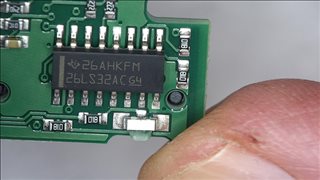
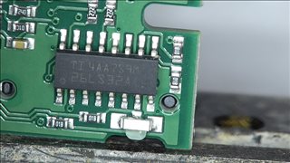
We have received AM26LS32ACDR ICs from a supplier, which have a supply current of approx. 5mA instead of the previous delivery, which had a supply current of approx. 50mA. According to the data sheet, the typical supply current is 52mA.
In addition, the imprint is different, among other things only the lettering “TI” can be seen instead of the Texas Instruments logo.
Can you tell me whether there has been a change on your part that explains the lower current consumption? And can it be an original component if the Texas Instruments logo is missing?

Many thanks for your help.

Kind regards
Andreas Schormair

  • Marking: PCN#20211123004.0
    New design: PCN#20230814006.1

    The new design is CMOS; it is probably identical with the AM26C32.

  • Thank you very much.

    This would be a possible cause.
    But why does the datasheet SLLS115G still lists a typical "ICC Supply current" of 52mA in chaper 6.5?

    And why is there no new designation of the component when the manufacturing process is changed?

  • Typical values are not guaranteed.

    The guaranteed datasheet limits have not changed.

  • As Clemens pointed out. The new device you have is likely the newly designed die we've made. You can see the PCN for details.

    To explain the current difference. The old design of the die was designed in the late 1970s. During this time, the semiconductor industry mainly designed using BJTs as this was a mature technology back then. BJTs are controlled by pushing current through the base, by using many of them the overall current consumption would be very large. I believe in the 90's CMOS technology had matured to the point where they were now more cost efficient than BJTs which shifted designers to use CMOS over BJTs. The biggest advantage (aside from cost) is that CMOS are voltage controlled on the gate. This results in very low current consumption since these gates are high impedance. The new dies for these devices were redesigned in the early 2020s which mainly consist of CMOS technology. This is why you see such a large difference between the old die and the new die.

    BJTs are still used today, but mainly for applications where bandwidth/frequency needs to be very fast (CMOS gates are capacitive and it takes more time to turn them on and off compared to BJTs). 

    But why does the datasheet SLLS115G still lists a typical "ICC Supply current" of 52mA in chaper 6.5?

    And why is there no new designation of the component when the manufacturing process is changed?

    TI's policy with electrical characteristics is to only change min/max values if they differ and issue a PCN when those values are changed. With typical values, these are not guaranteed. Customers are expected to design around min/max values so if a new design's characteristics are between the min/max then the application the previous die was designed in would still work with the newer die. Consumption current is one of those specs which lower is better and is not expected to cause a failure in new designs. 

    We issue PCNs to customers with the expectation that they evaluate the new dies in their system and validate the new dies work. 

    TI's move to replace the die is the alternative to EOL'ing the device since we are shutting down our fabs that still use the old process technology in favor or 300mm wafer technology. 

    -Bobby