This thread has been locked.

If you have a related question, please click the "Ask a related question" button in the top right corner. The newly created question will be automatically linked to this question.

DP83822H: Question about setup/hold time of TX_D[1:0] and TX_EN from/to XI rising.

Part Number: DP83822H

Tool/software:

Hello guys,

One of my customers is considering using DP83822H for their new products.

At this moment, they have the following question.
Could you please give me your reply?

Q.
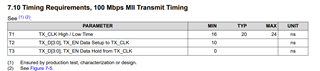
They are considering using this device with MII, 100BASE-TX.
and they want to know setup/hold time between XI(master clock input) and TX_D[1:0],TX_EN signal.

They found the following timing regulations for RMII case.
TX_D[1:0] and TX_EN Data Setup to XI rising
TX_D[1:0] and TX_EN Data Hold from XI rising

But they didn't find these regulation for MII case.

Could you please tell me these setup/hold timing regulation value?

Your reply would be much appreciated.

Best regards,
Kazuya.
  

  • Hi Kazuya-san,

    There are no setup/hold time values between XI and TX signals for MII because MII clock signals are both provided by the PHY as RX_CLK and TX_CLK. 

    For TX setup/hold times for MII, they can use T2 (10ns) as the setup time and T3 (0ns) as the hold time. However, please note that TX_CLK is also provided by the PHY. 


    Please let me know if you have additional questions. 

    Best,

    J

  • Hi J,

    Thank you very much for your reply.

    Could I ask you additional question?

    I understood the follow thing you wrote.

    >There are no setup/hold time values between XI and TX signals for MII because MII clock signals are both provided by the PHY as RX_CLK and TX_CLK. 

    My additional questions are the follows.

    Q1.
    TX_CLK and RX_CLK are always output from PHY as long as clock signal is input to XI pin?

    Q2.
    In general,  do TX_D[3:0] and TX_EN signal level from MAC side change at TX_CLK rising timing from PHY side?
    Or TX_CLK falling timing?

    Thank you again and best regards,
    Kazuya.

  • Hi J,

    Could I ask you one more question?

    Q3.
    Do you have any electrical characteristics data about delay time from XI rising edge input to TX_CLK rising edge output?

    Thank you very mu and best regards,
    Kazuya.

  • Hi Kazuya-san,

    Q1.
    TX_CLK and RX_CLK are always output from PHY as long as clock signal is input to XI pin?

    This is true.

    Q2.
    In general,  do TX_D[3:0] and TX_EN signal level from MAC side change at TX_CLK rising timing from PHY side?
    Or TX_CLK falling timing?

    The rising edge of TX_CLK.

    Q3.
    Do you have any electrical characteristics data about delay time from XI rising edge input to TX_CLK rising edge output?

    I will verify but I do not believe we have this data as MII signals are not impacted by XI signals because neither PHY or MAC can communicate until RX_CLK and TX_CLK are outputted.

    Best,

    J

  • Hi J,

    Thank you very much for your supports.

    In their system, DP83822H XI clock is supplied from MAC side.
    Also their MAC side doesn't have TX_CLK input pin.
    So they need the following data,
    TX_D[3:0], TX_EN Data Setup time to XI rising
    TX_D[3:0], TX_EN Data Hold time from XI rising
    or delay time from XI rising edge input to TX_CLK rising edge output.

    It doesn't matter for them if it's reference data that is not guaranteed.

    Your reply would be much appreciated.

    Thank you again and best regards,
    Kazuya. 

  • Hi Kazuya-san, 

    Because MII protocol dictates PHYs to use TX_CLK to clock the incoming data from the MAC, the MAC needs to have the TX_CLK to properly send data to the PHY. Without TX_CLK, there is unaccounted propagation delay internally from the PHY and to the MAC from the PHY and internally within the MAC since the MAC will send the data to the PHY. Using MAC's output clock to drive both XI and TX_D and TX_EN may have unaccounted ramifications. 

    Please let the customer know that we do not suggest this design. 

    Best,
    J