This thread has been locked.

If you have a related question, please click the "Ask a related question" button in the top right corner. The newly created question will be automatically linked to this question.

AFE7950EVM: I need information on the JESD input/output configuration of the AFE7950EVM board.

Part Number: AFE7950EVM
Other Parts Discussed in Thread: AFE7951,

Tool/software:

I am using AFE7950EVM and AFE7951 ICs

I need information on the JESD input/output configuration of the AFE7950EVM board.

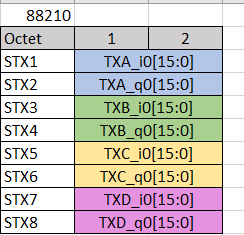
1. I want to know how the 8 inputs are mapped to each of the 4 DACs.
2. I want to know how the JESD data is configured for each input, which is a 14-bit DAC input.

For example, JESD is basically 8-bit, but to input 14-bit, do I need to input 8-bits twice (discarding the upper 2 bits) or do I need to input 8-bits to an input (say SRX1) and input 8-bits to another input (say SRX2) (discarding the upper 1 bit)?

  • Hi,

    1. The mapping of the data on the serdes lanes to the DACs is dependent on the LMFS being used. What is the LMFS that you are using?
    2. Resolution of RF DAC and ADC is 14-bits (real samples). But before interpolation and after decimation, SNR is higher due to bandpass filters in DUC and DDC. So 16-bit complex samples are used for baseband data.

    An example of the frame format for the LMFS 88210 is given below.

    Regards,

    David Chaparro 

  • Thank you

    I have additional questions

    1. Is there a way to connect AFE7951's DAC SYNCOUT1/SYNCOUT2/SYNCOUT3/SYNCOUT4 outputs to XCZU7EV FPGA device FMC connector?

    2. Is the ADC output of the AFE7951 represented as unsigned or signed integers?

    3. Is the DAC input of the AFE7951 represented as unsigned or signed integers?

    4. When RF signals are applied to the four ADCs of the AFE7951, how is the ADC output structured?

    • Are the ADCs outputting sequentially, 8 bits each?
      (e.g., 8-bit output from ADC_1 → ADC_2 → ADC_3 → ADC_4)

    • Or do all 4 ADCs output data simultaneously in serial format?
      If it is serial, how are the 8 output ports connected?

    5. How is input data applied to the four DACs of the AFE7951?

    • Do we need to input 8 bits sequentially to each DAC?
      (e.g., 8-bit input to DAC_1 → DAC_2 → DAC_3 → DAC_4)

    • Or should all 4 DACs receive input simultaneously in serial format?
      If so, to which input ports should the serial data be connected?

    Regards

  • Hi,

    1. The ADCs and DACs are typically used in a single JESD link so you would only need to connect one of the SYNC signals to the FPGA. The SYNC signal is connected to the FMC. Please see the EVM schematic for further details.

    2. Signed integers.

    3. Signed integers.

    4. All ADCs are sampled simultaneously. After the DDC the samples are 16bits and the packing would follow the frame format shown in my previous response. 

    5. 16 bit samples should be provided in the frame format given in my first response.

    Regards,

    David Chaparro