Part Number: TUSB319-Q1
Other Parts Discussed in Thread: TUSB320, TUSB319EVM, HD3SS3220
Tool/software:
Hello all,
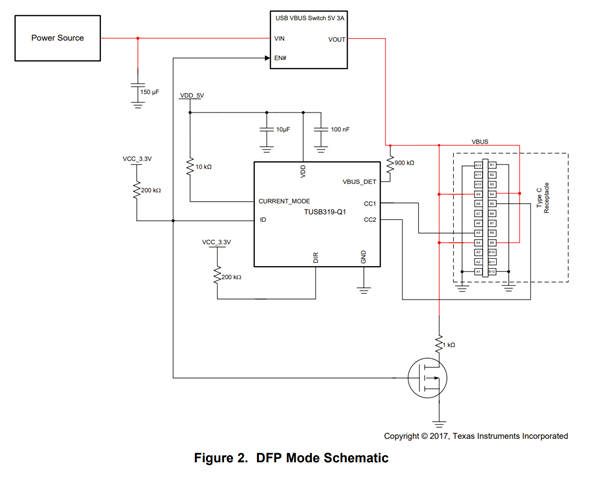
I’m reviewing the TUSB319 datasheet (page 10), and I noticed that the schematic places the required 150 µF bulk capacitor before the load switch (i.e., between VBUS and the load switch input), as required by the USB PD specification.
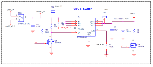
However, when looking at the TUSB319 evaluation board schematic, the bulk capacitor is placed after the load switch (i.e., at the output).
This raises a question: which placement is correct or recommended?
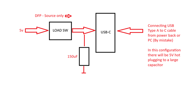
My concern is that placing the bulk capacitor after the load switch could result in a huge inrush current if someone mistakenly connects a USB Type-A to Type-C cable to this port. In such a case, VBUS would already be present on the cable (i.e., hot plug), unlike a USB-C to USB-C connection where power negotiation would occur first.
Has anyone else run into this or have a different perspective?
Thanks,
Nir