Other Parts Discussed in Thread: ADS131M04,
Tool/software:
Dear team,
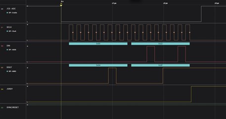
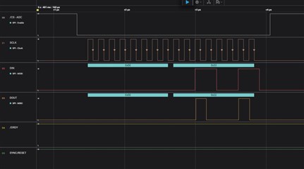
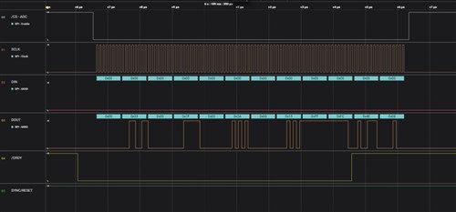
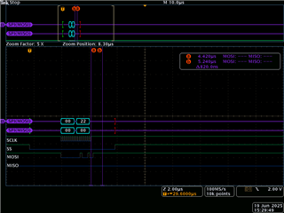
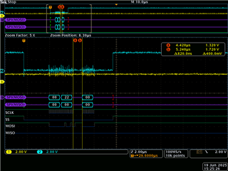
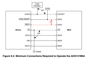
I have interfaced ADS131m04 with MCU with below hw connection, only thing is
1. CLKIN pin of ADS131 from Connector I have kept open, since i need it from local oscillator. Should i have to externally connect from JP6 to CLKIN?
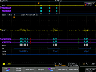
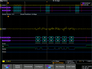
2. SYNC/RESET & DRDY, i have connected it to GPIO & below is the GPIO config from MCU side
For DRDY, GPIO configured as digital Input pin, pull up enabled, fast slew rate, passive filter disabled, Low drive strength & interrupt enabled on falling edge.
For SYNC/RESET, GPIO configured as digital Output pin, pull up enabled, fast slew rate, passive filter disabled, Low drive strength.
3. SPI initialisation done.
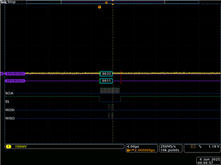
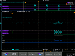
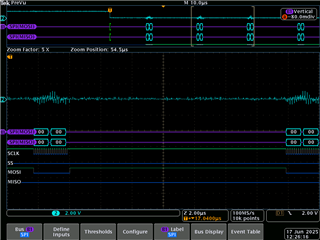
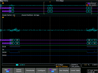
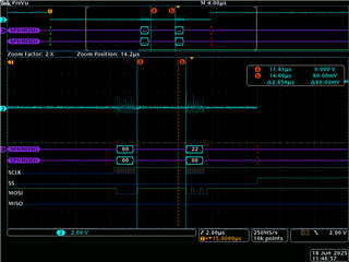
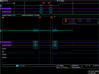
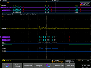
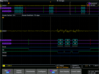
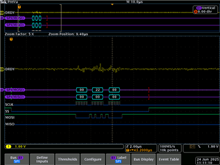
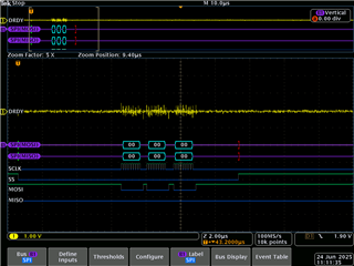
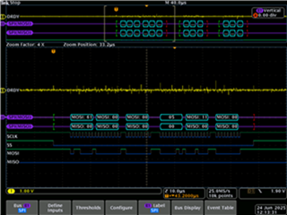
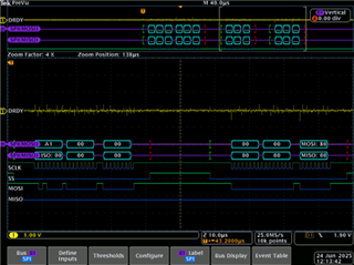
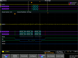
ADC initialization is not happening, also DRDY pin interrupt i get only once & the pin always remains low after that. Here if I monitor the DRDY pin on scope, at startup i get DRDY High(1.2V), after that only one inerrupt is raised & pin status goes from 1.2V to 1V & it remains stable at 1V & there is no interrupt observed on this pin later on.
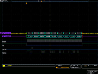
On SPI lines, I can see some data on MOSI but not on MISO.
Anything i am missing here?
ADC startup, lib file i have attached below
/**
 * \copyright Copyright (C) 2019 Texas Instruments Incorporated - http://www.ti.com/
 *
 *  Redistribution and use in source and binary forms, with or without
 *  modification, are permitted provided that the following conditions
 *  are met:
 *
 *    Redistributions of source code must retain the above copyright
 *    notice, this list of conditions and the following disclaimer.
 *
 *    Redistributions in binary form must reproduce the above copyright
 *    notice, this list of conditions and the following disclaimer in the
 *    documentation and/or other materials provided with the
 *    distribution.
 *
 *    Neither the name of Texas Instruments Incorporated nor the names of
 *    its contributors may be used to endorse or promote products derived
 *    from this software without specific prior written permission.
 *
 *  THIS SOFTWARE IS PROVIDED BY THE COPYRIGHT HOLDERS AND CONTRIBUTORS
 *  "AS IS" AND ANY EXPRESS OR IMPLIED WARRANTIES, INCLUDING, BUT NOT
 *  LIMITED TO, THE IMPLIED WARRANTIES OF MERCHANTABILITY AND FITNESS FOR
 *  A PARTICULAR PURPOSE ARE DISCLAIMED. IN NO EVENT SHALL THE COPYRIGHT
 *  OWNER OR CONTRIBUTORS BE LIABLE FOR ANY DIRECT, INDIRECT, INCIDENTAL,
 *  SPECIAL, EXEMPLARY, OR CONSEQUENTIAL DAMAGES (INCLUDING, BUT NOT
 *  LIMITED TO, PROCUREMENT OF SUBSTITUTE GOODS OR SERVICES; LOSS OF USE,
 *  DATA, OR PROFITS; OR BUSINESS INTERRUPTION) HOWEVER CAUSED AND ON ANY
 *  THEORY OF LIABILITY, WHETHER IN CONTRACT, STRICT LIABILITY, OR TORT
 *  (INCLUDING NEGLIGENCE OR OTHERWISE) ARISING IN ANY WAY OUT OF THE USE
 *  OF THIS SOFTWARE, EVEN IF ADVISED OF THE POSSIBILITY OF SUCH DAMAGE.
 *
 */

#include "ads131m0x.h"


//****************************************************************************
//
// Internal variables
//
//****************************************************************************

// Array used to recall device register map configurations */
static uint16_t             registerMap[NUM_REGISTERS];

// Array of SPI word lengths
const static uint8_t        wlength_byte_values[] = {2, 3, 4, 4};


//****************************************************************************
//
// Internal function prototypes
//
//****************************************************************************

uint8_t     buildSPIarray(const uint16_t opcodeArray[], uint8_t numberOpcodes, uint8_t byteArray[]);
uint16_t    enforce_selected_device_modes(uint16_t data);
uint8_t     getWordByteLength(void);


//*****************************************************************************
//
//! Getter function to access registerMap array from outside of this module.
//!
//! \fn uint16_t getRegisterValue(uint8_t address)
//!
//! NOTE: The internal registerMap arrays stores the last know register value,
//! since the last read or write operation to that register. This function
//! does not communicate with the device to retrieve the current register value.
//! For the most up-to-date register data or retrieving the value of a hardware
//! controlled register, it is recommend to use readSingleRegister() to read the
//! current register value.
//!
//! \return unsigned 16-bit register value.
//
//*****************************************************************************
uint16_t getRegisterValue(uint8_t address)
{
    assert(address < NUM_REGISTERS);
    return registerMap[address];
}


//*****************************************************************************
//
//! Example start up sequence for the ADS131M0x.
//!
//! \fn void adcStartup(void)
//!
//! Before calling this function, the device must be powered,
//! the SPI/GPIO pins of the MCU must have already been configured,
//! and (if applicable) the external clock source should be provided to CLKIN.
//!
//! \return None.
//
//*****************************************************************************
void adcStartup(void)
{
	/* (OPTIONAL) Provide additional delay time for power supply settling */
	delay_ms(50);

	/* (REQUIRED) Set nRESET pin high for ADC operation */
	setSYNC_RESET(HIGH);

	/* (OPTIONAL) Toggle nRESET pin to ensure default register settings. */
	/* NOTE: This also ensures that the device registers are unlocked.	 */
	toggleRESET();

    /* (REQUIRED) Initialize internal 'registerMap' array with device default settings */
	restoreRegisterDefaults();

    /* (OPTIONAL) Validate first response word when beginning SPI communication: (0xFF20 | CHANCNT) */
	uint16_t response = sendCommand(OPCODE_NULL);

	/* (OPTIONAL) Define your initial register settings here */
    writeSingleRegister(CLOCK_ADDRESS, (CLOCK_DEFAULT & ~CLOCK_OSR_MASK) | CLOCK_OSR_256);

    /* (REQUIRED) Configure MODE register settings
     * NOTE: This function call is required here for this particular code implementation to work.
     * This function will enforce the MODE register settings as selected in the 'ads131m0x.h' header file.
     */
    writeSingleRegister(MODE_ADDRESS, MODE_DEFAULT);

    /* (OPTIONAL) Read back all registers */

	/* (OPTIONAL) Check STATUS register for faults */
}


//*****************************************************************************
//
//! Reads the contents of a single register at the specified address.
//!
//! \fn uint16_t readSingleRegister(uint8_t address)
//!
//! \param address is the 8-bit address of the register to read.
//!
//! \return Returns the 8-bit register read result.
//
//*****************************************************************************
uint16_t readSingleRegister(uint8_t address)
{
	/* Check that the register address is in range */
	assert(address < NUM_REGISTERS);

// Build TX and RX byte array
#ifdef ENABLE_CRC_IN
    uint8_t dataTx[8] = { 0 };      // 2 words, up to 4 bytes each = 8 bytes maximum
    uint8_t dataRx[8] = { 0 };
#else
    uint8_t dataTx[4] = { 0 };      // 1 word, up to 4 bytes long = 4 bytes maximum
    uint8_t dataRx[4] = { 0 };
#endif
    uint16_t opcode = OPCODE_RREG | (((uint16_t) address) << 7);
    uint8_t numberOfBytes = buildSPIarray(&opcode, 1, dataTx);

	// [FRAME 1] Send RREG command
	spiSendReceiveArrays(dataTx, dataRx, numberOfBytes);

	// [FRAME 2] Send NULL command to retrieve the register data
	registerMap[address] = sendCommand(OPCODE_NULL);

	return registerMap[address];
}


//*****************************************************************************
//
//! Writes data to a single register.
//!
//! \fn void writeSingleRegister(uint8_t address, uint16_t data)
//!
//! \param address is the address of the register to write to.
//! \param data is the value to write.
//!
//! This command will be ignored if device registers are locked.
//!
//! \return None.
//
//*****************************************************************************
void writeSingleRegister(uint8_t address, uint16_t data)
{
    /* Check that the register address is in range */
    assert(address < NUM_REGISTERS);

    // (OPTIONAL) Enforce certain register field values when
    // writing to the MODE register to fix the operation mode
    if (MODE_ADDRESS == address)
    {
        data = enforce_selected_device_modes(data);
    }

    // Build TX and RX byte array
#ifdef ENABLE_CRC_IN
    uint8_t dataTx[12] = { 0 };     // 3 words, up to 4 bytes each = 12 bytes maximum
    uint8_t dataRx[12] = { 0 };
#else
    uint8_t dataTx[8] = { 0 };      // 2 words, up to 4 bytes long = 8 bytes maximum
    uint8_t dataRx[8] = { 0 };
#endif
    uint16_t opcodes[2];
    opcodes[0] = OPCODE_WREG | (((uint16_t) address) << 7);
    opcodes[1] = data;
    uint8_t numberOfBytes = buildSPIarray(&opcodes[0], 2, dataTx);

    // Send command
    spiSendReceiveArrays(dataTx, dataRx, numberOfBytes);

    // Update internal array
    registerMap[address] = data;

    // (RECOMMENDED) Read back register to confirm register write was successful
    readSingleRegister(address);

    // NOTE: Enabling the CRC words in the SPI command will NOT prevent an invalid W
}


//*****************************************************************************
//
//! Reads ADC data.
//!
//! \fn bool readData(adc_channel_data *DataStruct)
//!
//! \param *DataStruct points to an adc_channel_data type-defined structure/
//!
//! NOTE: Should be called after /DRDY goes low, and not during a /DRDY falling edge!
//!
//! \return Returns true if the CRC-OUT of the data read detects an error.
//
//*****************************************************************************
bool readData(adc_channel_data *DataStruct)
{
    int i;
    uint8_t crcTx[4]                        = { 0 };
    uint8_t dataRx[4]                       = { 0 };
    uint8_t bytesPerWord                    = getWordByteLength();

#ifdef ENABLE_CRC_IN
    // Build CRC word (only if "RX_CRC_EN" register bit is enabled)
    uint16_t crcWordIn = calculateCRC(&DataTx[0], bytesPerWord * 2, 0xFFFF);
    crcTx[0] = upperByte(crcWordIn);
    crcTx[1] = lowerByte(crcWordIn);
#endif

    /* Set the nCS pin LOW */
    setCS(LOW);

    // Send NULL word, receive response word
    for (i = 0; i < bytesPerWord; i++)
    {
        dataRx[i] = spiSendReceiveByte(0x00);
    }
    DataStruct->response = combineBytes(dataRx[0], dataRx[1]);

    // (OPTIONAL) Do something with the response (STATUS) word.
    // ...Here we only use the response for calculating the CRC-OUT
    //uint16_t crcWord = calculateCRC(&dataRx[0], bytesPerWord, 0xFFFF);

    // (OPTIONAL) Ignore CRC error checking
    uint16_t crcWord = 0;

    // Send 2nd word, receive channel 1 data
    for (i = 0; i < bytesPerWord; i++)
    {
        dataRx[i] = spiSendReceiveByte(crcTx[i]);
    }
    DataStruct->channel0 = signExtend(&dataRx[0]);
    //crcWord = calculateCRC(&dataRx[0], bytesPerWord, crcWord);

#if (CHANNEL_COUNT > 1)

    // Send 3rd word, receive channel 2 data
    for (i = 0; i < bytesPerWord; i++)
    {
        dataRx[i] = spiSendReceiveByte(0x00);
    }
    DataStruct->channel1 = signExtend(&dataRx[0]);
    //crcWord = calculateCRC(&dataRx[0], bytesPerWord, crcWord);

#endif
#if (CHANNEL_COUNT > 2)

    // Send 4th word, receive channel 3 data
    for (i = 0; i < bytesPerWord; i++)
    {
        dataRx[i] = spiSendReceiveByte(0x00);
    }
    DataStruct->channel2 = signExtend(&dataRx[0]);
    //crcWord = calculateCRC(&dataRx[0], bytesPerWord, crcWord);

#endif
#if (CHANNEL_COUNT > 3)

    // Send 5th word, receive channel 4 data
    for (i = 0; i < bytesPerWord; i++)
    {
        dataRx[i] = spiSendReceiveByte(0x00);
    }
    DataStruct->channel3 = signExtend(&dataRx[0]);
    //crcWord = calculateCRC(&dataRx[0], bytesPerWord, crcWord);

#endif
#if (CHANNEL_COUNT > 4)

    // Send 6th word, receive channel 5 data
    for (i = 0; i < bytesPerWord; i++)
    {
        dataRx[i] = spiSendReceiveByte(0x00);
    }
    DataStruct->channel4 = signExtend(&dataRx[0]);
    //crcWord = calculateCRC(&dataRx[0], bytesPerWord, crcWord);

#endif
#if (CHANNEL_COUNT > 5)

    // Send 7th word, receive channel 6 data
    for (i = 0; i < bytesPerWord; i++)
    {
        dataRx[i] = spiSendReceiveByte(0x00);
    }
    DataStruct->channel5 = signExtend(&dataRx[0]);
    //crcWord = calculateCRC(&dataRx[0], bytesPerWord, crcWord);

#endif
#if (CHANNEL_COUNT > 6)

    // Send 8th word, receive channel 7 data
    for (i = 0; i < bytesPerWord; i++)
    {
        dataRx[i] = spiSendReceiveByte(0x00);
    }
    DataStruct->channel6 = signExtend(&dataRx[0]);
    //crcWord = calculateCRC(&dataRx[0], bytesPerWord, crcWord);

#endif
#if (CHANNEL_COUNT > 7)

    // Send 9th word, receive channel 8 data
    for (i = 0; i < bytesPerWord; i++)
    {
        dataRx[i] = spiSendReceiveByte(0x00);
    }
    DataStruct->channel7 = signExtend(&dataRx[0]);
    //crcWord = calculateCRC(&dataRx[0], bytesPerWord, crcWord);

#endif

    // Send the next word, receive CRC data
    for (i = 0; i < bytesPerWord; i++)
    {
        dataRx[i] = spiSendReceiveByte(0x00);
    }
    DataStruct->crc = combineBytes(dataRx[0], dataRx[1]);

    /* NOTE: If we continue calculating the CRC with a matching CRC, the result should be zero.
     * Any non-zero result will indicate a mismatch.
     */
    //crcWord = calculateCRC(&dataRx[0], bytesPerWord, crcWord);

    /* Set the nCS pin HIGH */
    setCS(HIGH);

    // Returns true when a CRC error occurs
    return ((bool) crcWord);
}


//*****************************************************************************
//
//! Sends the specified SPI command to the ADC (NULL, STANDBY, or WAKEUP).
//!
//! \fn uint16_t sendCommand(uint16_t opcode)
//!
//! \param opcode SPI command byte.
//!
//! NOTE: Other commands have their own dedicated functions to support
//! additional functionality.
//!
//! \return ADC response byte (typically the STATUS byte).
//
//*****************************************************************************
uint16_t sendCommand(uint16_t opcode)
{
    /* Assert if this function is used to send any of the following opcodes */
    assert(OPCODE_RREG != opcode);      /* Use "readSingleRegister()"   */
    assert(OPCODE_WREG != opcode);      /* Use "writeSingleRegister()"  */
    assert(OPCODE_LOCK != opcode);      /* Use "lockRegisters()"        */
    assert(OPCODE_UNLOCK != opcode);    /* Use "unlockRegisters()"      */
    assert(OPCODE_RESET != opcode);     /* Use "resetDevice()"          */

    // Build TX and RX byte array
#ifdef ENABLE_CRC_IN
    uint8_t dataTx[8] = { 0 };      // 2 words, up to 4 bytes each = 8 bytes maximum
    uint8_t dataRx[8] = { 0 };
#else
    uint8_t dataTx[4] = { 0 };      // 1 word, up to 4 bytes long = 4 bytes maximum
    uint8_t dataRx[4] = { 0 };
#endif
    uint8_t numberOfBytes = buildSPIarray(&opcode, 1, dataTx);

    /* Set the nCS pin LOW */
    setCS(LOW);

    // Send the opcode (and crc word, if enabled)
    int i;
    for (i = 0; i < numberOfBytes; i++)
    {
       dataRx[i] = spiSendReceiveByte(dataTx[i]);
    }

    /* Set the nCS pin HIGH */
    setCS(HIGH);

    // Combine response bytes and return as a 16-bit word
    uint16_t adcResponse = combineBytes(dataRx[0], dataRx[1]);
    return adcResponse;
}


//*****************************************************************************
//
//! Resets the device.
//!
//! \fn void resetDevice(void)
//!
//! NOTE: This function does not capture DOUT data, but it could be modified
//! to do so.
//!
//! \return None.
//
//*****************************************************************************
void resetDevice(void)
{
    // Build TX and RX byte array
#ifdef ENABLE_CRC_IN
    uint8_t dataTx[8] = { 0 };      // 2 words, up to 4 bytes each = 8 bytes maximum
    //uint8_t dataRx[8] = { 0 };    // Only needed if capturing data
#else
    uint8_t dataTx[4] = { 0 };      // 1 word, up to 4 bytes long = 4 bytes maximum
    //uint8_t dataRx[4] = { 0 };    // Only needed if capturing data
#endif
    uint16_t opcode         = OPCODE_RESET;
    uint8_t numberOfBytes   = buildSPIarray(&opcode, 1, dataTx);

    uint8_t bytesPerWord    = wlength_byte_values[WLENGTH];
    uint8_t wordsInFrame    = CHANNEL_COUNT + 2;

    // Set the nCS pin LOW
    setCS(LOW);

    // Send the opcode (and CRC word, if enabled)
    int i;
    for (i = 0; i < numberOfBytes; i++)
    {
         spiSendReceiveByte(dataTx[i]);
    }

    // Finish sending remaining bytes
    for (i = numberOfBytes; i < (wordsInFrame * bytesPerWord); i++)
    {
        spiSendReceiveByte(0x00);
    }

    // NOTE: The ADS131M0x's next response word should be (0xFF20 | CHANCNT),
    // if the response is 0x0011 (acknowledge of RESET command), then the device
    // did not receive a full SPI frame and the reset did not occur!

    // Set the nCS pin HIGH
    setCS(HIGH);

    // tSRLRST delay, ~1ms with 2.048 MHz fCLK
    delay_ms(1);

    // Update register setting array to keep software in sync with device
    restoreRegisterDefaults();

    // Write to MODE register to enforce mode settings
    writeSingleRegister(MODE_ADDRESS, MODE_DEFAULT);
}


//*****************************************************************************
//
//! Sends the LOCK command and verifies that registers are locked.
//!
//! \fn bool lockRegisters(void)
//!
//! \return boolean to indicate if an error occurred (0 = no error; 1 = error)
//
//*****************************************************************************
bool lockRegisters(void)
{
    bool b_lock_error;

    // Build TX and RX byte array
#ifdef ENABLE_CRC_IN
    uint8_t dataTx[8] = { 0 };      // 2 words, up to 4 bytes each = 8 bytes maximum
    uint8_t dataRx[8] = { 0 };
#else
    uint8_t dataTx[4] = { 0 };      // 1 word, up to 4 bytes long = 4 bytes maximum
    uint8_t dataRx[4] = { 0 };
#endif
    uint16_t opcode         = OPCODE_LOCK;
    uint8_t numberOfBytes   = buildSPIarray(&opcode, 1, dataTx);

    // Send command
    spiSendReceiveArrays(dataTx, dataRx, numberOfBytes);

    /* (OPTIONAL) Check for SPI errors by sending the NULL command and checking STATUS */

    /* (OPTIONAL) Read back the STATUS register and check if LOCK bit is set... */
    readSingleRegister(STATUS_ADDRESS);
    if (!SPI_LOCKED) { b_lock_error = true; }

    /* If the STATUS register is NOT read back,
     * then make sure to manually update the global register map variable... */
    //registerMap[STATUS_ADDRESS]  |= STATUS_LOCK_LOCKED;

    /* (OPTIONAL) Error handler */
    if (b_lock_error)
    {
        // Insert error handler function call here...
    }

    return b_lock_error;
}


//*****************************************************************************
//
//! Sends the UNLOCK command and verifies that registers are unlocked
//!
//! \fn bool unlockRegisters(void)
//!
//! \return boolean to indicate if an error occurred (0 = no error; 1 = error)
//
//*****************************************************************************
bool unlockRegisters(void)
{
	bool b_unlock_error;

    // Build TX and RX byte array
#ifdef ENABLE_CRC_IN
    uint8_t dataTx[8] = { 0 };      // 2 words, up to 4 bytes each = 8 bytes maximum
    uint8_t dataRx[8] = { 0 };
#else
    uint8_t dataTx[4] = { 0 };      // 1 word, up to 4 bytes long = 4 bytes maximum
    uint8_t dataRx[4] = { 0 };
#endif
    uint16_t opcode = OPCODE_UNLOCK;
    uint8_t numberOfBytes = buildSPIarray(&opcode, 1, dataTx);

    // Send command
    spiSendReceiveArrays(dataTx, dataRx, numberOfBytes);

    /* (OPTIONAL) Check for SPI errors by sending the NULL command and checking STATUS */

    /* (OPTIONAL) Read the STATUS register and check if LOCK bit is cleared... */
    readSingleRegister(STATUS_ADDRESS);
    if (SPI_LOCKED) { b_unlock_error = true; }

    /* If the STATUS register is NOT read back,
     * then make sure to manually update the global register map variable... */
    //registerMap[STATUS_ADDRESS]  &= !STATUS_LOCK_LOCKED;

    /* (OPTIONAL) Error handler */
    if (b_unlock_error)
    {
        // Insert error handler function call here...
    }

    return b_unlock_error;
}


//*****************************************************************************
//
//! Calculates the 16-bit CRC for the selected CRC polynomial.
//!
//! \fn uint16_t calculateCRC(const uint8_t dataBytes[], uint8_t numberBytes, uint16_t initialValue)
//!
//! \param dataBytes[] pointer to first element in the data byte array
//! \param numberBytes number of bytes to be used in CRC calculation
//! \param initialValue the seed value (or partial crc calculation), use 0xFFFF when beginning a new CRC computation
//!
//! NOTE: This calculation is shown as an example and is not optimized for speed.
//!
//! \return 16-bit calculated CRC word
//
//*****************************************************************************
uint16_t calculateCRC(const uint8_t dataBytes[], uint8_t numberBytes, uint16_t initialValue)
{
	/* Check that "dataBytes" is not a null pointer */
	assert(dataBytes != 0x00);

	int         bitIndex, byteIndex;
	bool        dataMSb;						/* Most significant bit of data byte */
	bool        crcMSb;						    /* Most significant bit of crc byte  */
	uint8_t     bytesPerWord = wlength_byte_values[WLENGTH];

	/*
     * Initial value of crc register
     * NOTE: The ADS131M0x defaults to 0xFFFF,
     * but can be set at function call to continue an on-going calculation
     */
    uint16_t crc = initialValue;

    #ifdef CRC_CCITT
    /* CCITT CRC polynomial = x^16 + x^12 + x^5 + 1 */
    const uint16_t poly = 0x1021;
    #endif

    #ifdef CRC_ANSI
    /* ANSI CRC polynomial = x^16 + x^15 + x^2 + 1 */
    const uint16_t poly = 0x8005;
    #endif

    //
    // CRC algorithm
    //

    // Loop through all bytes in the dataBytes[] array
	for (byteIndex = 0; byteIndex < numberBytes; byteIndex++)
	{
	    // Point to MSb in byte
	    bitIndex = 0x80u;

	    // Loop through all bits in the current byte
	    while (bitIndex > 0)
	    {
	        // Check MSB's of data and crc
	        dataMSb = (bool) (dataBytes[byteIndex] & bitIndex);
	        crcMSb  = (bool) (crc & 0x8000u);

	        crc <<= 1;              /* Left shift CRC register */

	        // Check if XOR operation of MSBs results in additional XOR operations
	        if (dataMSb ^ crcMSb)
	        {
	            crc ^= poly;        /* XOR crc with polynomial */
	        }

	        /* Shift MSb pointer to the next data bit */
	        bitIndex >>= 1;
	    }
	}

	return crc;
}


//*****************************************************************************
//
//! Updates the registerMap[] array to its default values.
//!
//! \fn void restoreRegisterDefaults(void)
//!
//! NOTES:
//! - If the MCU keeps a copy of the ADS131M0x register settings in memory,
//! then it is important to ensure that these values remain in sync with the
//! actual hardware settings. In order to help facilitate this, this function
//! should be called after powering up or resetting the device (either by
//! hardware pin control or SPI software command).
//!
//! - Reading back all of the registers after resetting the device can
//! accomplish the same result; however, this might be problematic if the
//! device was previously in CRC mode or the WLENGTH was modified, since
//! resetting the device exits these modes. If the MCU is not aware of this
//! mode change, then read register commands will return invalid data due to
//! the expectation of data appearing in a different byte position.
//!
//! \return None.
//
//*****************************************************************************
void restoreRegisterDefaults(void)
{
    registerMap[ID_ADDRESS]             =   0x00;               /* NOTE: This a read-only register */
    registerMap[STATUS_ADDRESS]         =   STATUS_DEFAULT;
    registerMap[MODE_ADDRESS]           =   MODE_DEFAULT;
    registerMap[CLOCK_ADDRESS]          =   CLOCK_DEFAULT;
    registerMap[GAIN1_ADDRESS]          =   GAIN1_DEFAULT;
    registerMap[GAIN2_ADDRESS]          =   GAIN2_DEFAULT;
    registerMap[CFG_ADDRESS]            =   CFG_DEFAULT;
    registerMap[THRSHLD_MSB_ADDRESS]    =   THRSHLD_MSB_DEFAULT;
    registerMap[THRSHLD_LSB_ADDRESS]    =   THRSHLD_LSB_DEFAULT;
    registerMap[CH0_CFG_ADDRESS]        =   CH0_CFG_DEFAULT;
    registerMap[CH0_OCAL_MSB_ADDRESS]   =   CH0_OCAL_MSB_DEFAULT;
    registerMap[CH0_OCAL_LSB_ADDRESS]   =   CH0_OCAL_LSB_DEFAULT;
    registerMap[CH0_GCAL_MSB_ADDRESS]   =   CH0_GCAL_MSB_DEFAULT;
    registerMap[CH0_GCAL_LSB_ADDRESS]   =   CH0_GCAL_LSB_DEFAULT;
#if (CHANNEL_COUNT > 1)
    registerMap[CH1_CFG_ADDRESS]        =   CH1_CFG_DEFAULT;
    registerMap[CH1_OCAL_MSB_ADDRESS]   =   CH1_OCAL_MSB_DEFAULT;
    registerMap[CH1_OCAL_LSB_ADDRESS]   =   CH1_OCAL_LSB_DEFAULT;
    registerMap[CH1_GCAL_MSB_ADDRESS]   =   CH1_GCAL_MSB_DEFAULT;
    registerMap[CH1_GCAL_LSB_ADDRESS]   =   CH1_GCAL_LSB_DEFAULT;
#endif
#if (CHANNEL_COUNT > 2)
    registerMap[CH2_CFG_ADDRESS]        =   CH2_CFG_DEFAULT;
    registerMap[CH2_OCAL_MSB_ADDRESS]   =   CH2_OCAL_MSB_DEFAULT;
    registerMap[CH2_OCAL_LSB_ADDRESS]   =   CH2_OCAL_LSB_DEFAULT;
    registerMap[CH2_GCAL_MSB_ADDRESS]   =   CH2_GCAL_MSB_DEFAULT;
    registerMap[CH2_GCAL_LSB_ADDRESS]   =   CH2_GCAL_LSB_DEFAULT;
#endif
#if (CHANNEL_COUNT > 3)
    registerMap[CH3_CFG_ADDRESS]        =   CH3_CFG_DEFAULT;
    registerMap[CH3_OCAL_MSB_ADDRESS]   =   CH3_OCAL_MSB_DEFAULT;
    registerMap[CH3_OCAL_LSB_ADDRESS]   =   CH3_OCAL_LSB_DEFAULT;
    registerMap[CH3_GCAL_MSB_ADDRESS]   =   CH3_GCAL_MSB_DEFAULT;
    registerMap[CH3_GCAL_LSB_ADDRESS]   =   CH3_GCAL_LSB_DEFAULT;
#endif
#if (CHANNEL_COUNT > 4)
    registerMap[CH4_CFG_ADDRESS]        =   CH4_CFG_DEFAULT;
    registerMap[CH4_OCAL_MSB_ADDRESS]   =   CH4_OCAL_MSB_DEFAULT;
    registerMap[CH4_OCAL_LSB_ADDRESS]   =   CH4_OCAL_LSB_DEFAULT;
    registerMap[CH4_GCAL_MSB_ADDRESS]   =   CH4_GCAL_MSB_DEFAULT;
    registerMap[CH4_GCAL_LSB_ADDRESS]   =   CH4_GCAL_LSB_DEFAULT;
#endif
#if (CHANNEL_COUNT > 5)
    registerMap[CH5_CFG_ADDRESS]        =   CH5_CFG_DEFAULT;
    registerMap[CH5_OCAL_MSB_ADDRESS]   =   CH5_OCAL_MSB_DEFAULT;
    registerMap[CH5_OCAL_LSB_ADDRESS]   =   CH5_OCAL_LSB_DEFAULT;
    registerMap[CH5_GCAL_MSB_ADDRESS]   =   CH5_GCAL_MSB_DEFAULT;
    registerMap[CH5_GCAL_LSB_ADDRESS]   =   CH5_GCAL_LSB_DEFAULT;
#endif
#if (CHANNEL_COUNT > 6)
    registerMap[CH6_CFG_ADDRESS]        =   CH6_CFG_DEFAULT;
    registerMap[CH6_OCAL_MSB_ADDRESS]   =   CH6_OCAL_MSB_DEFAULT;
    registerMap[CH6_OCAL_LSB_ADDRESS]   =   CH6_OCAL_LSB_DEFAULT;
    registerMap[CH6_GCAL_MSB_ADDRESS]   =   CH6_GCAL_MSB_DEFAULT;
    registerMap[CH6_GCAL_LSB_ADDRESS]   =   CH6_GCAL_LSB_DEFAULT;
#endif
#if (CHANNEL_COUNT > 7)
    registerMap[CH7_CFG_ADDRESS]        =   CH7_CFG_DEFAULT;
    registerMap[CH7_OCAL_MSB_ADDRESS]   =   CH7_OCAL_MSB_DEFAULT;
    registerMap[CH7_OCAL_LSB_ADDRESS]   =   CH7_OCAL_LSB_DEFAULT;
    registerMap[CH7_GCAL_MSB_ADDRESS]   =   CH7_GCAL_MSB_DEFAULT;
    registerMap[CH7_GCAL_LSB_ADDRESS]   =   CH7_GCAL_LSB_DEFAULT;
#endif
    registerMap[REGMAP_CRC_ADDRESS]     =   REGMAP_CRC_DEFAULT;
}


//****************************************************************************
//
// Helper functions
//
//****************************************************************************


//*****************************************************************************
//
//! Takes a 16-bit word and returns the most-significant byte.
//!
//! \fn uint8_t upperByte(uint16_t uint16_Word)
//!
//! \param temp_word is the original 16-bit word.
//!
//! \return 8-bit most-significant byte.
//
//*****************************************************************************
uint8_t upperByte(uint16_t uint16_Word)
{
    uint8_t msByte;
    msByte = (uint8_t) ((uint16_Word >> 8) & 0x00FF);

    return msByte;
}


//*****************************************************************************
//
//! Takes a 16-bit word and returns the least-significant byte.
//!
//! \fn uint8_t lowerByte(uint16_t uint16_Word)
//!
//! \param temp_word is the original 16-bit word.
//!
//! \return 8-bit least-significant byte.
//
//*****************************************************************************
uint8_t lowerByte(uint16_t uint16_Word)
{
    uint8_t lsByte;
    lsByte = (uint8_t) (uint16_Word & 0x00FF);

    return lsByte;
}


//*****************************************************************************
//
//! Takes two 8-bit words and returns a concatenated 16-bit word.
//!
//! \fn uint16_t combineBytes(uint8_t upperByte, uint8_t lowerByte)
//!
//! \param upperByte is the 8-bit value that will become the MSB of the 16-bit word.
//! \param lowerByte is the 8-bit value that will become the LSB of the 16-bit word.
//!
//! \return concatenated 16-bit word.
//
//*****************************************************************************
uint16_t combineBytes(uint8_t upperByte, uint8_t lowerByte)
{
    uint16_t combinedValue;
    combinedValue = ((uint16_t) upperByte << 8) | ((uint16_t) lowerByte);

    return combinedValue;
}


//*****************************************************************************
//
//! Combines ADC data bytes into a single signed 32-bit word.
//!
//! \fn int32_t combineDataBytes(const uint8_t dataBytes[])
//!
//! \param dataBytes is a pointer to uint8_t[] where the first element is the MSB.
//!
//! \return Returns the signed-extend 32-bit result.
//
//*****************************************************************************
int32_t signExtend(const uint8_t dataBytes[])
{

#ifdef WORD_LENGTH_24BIT

    int32_t upperByte   = ((int32_t) dataBytes[0] << 24);
    int32_t middleByte  = ((int32_t) dataBytes[1] << 16);
    int32_t lowerByte   = ((int32_t) dataBytes[2] << 8);

    return (((int32_t) (upperByte | middleByte | lowerByte)) >> 8);     // Right-shift of signed data maintains signed bit

#elif defined WORD_LENGTH_32BIT_SIGN_EXTEND

    int32_t signByte    = ((int32_t) dataBytes[0] << 24);
    int32_t upperByte   = ((int32_t) dataBytes[1] << 16);
    int32_t middleByte  = ((int32_t) dataBytes[2] << 8);
    int32_t lowerByte   = ((int32_t) dataBytes[3] << 0);

    return (signByte | upperByte | middleByte | lowerByte);

#elif defined WORD_LENGTH_32BIT_ZERO_PADDED

    int32_t upperByte   = ((int32_t) dataBytes[0] << 24);
    int32_t middleByte  = ((int32_t) dataBytes[1] << 16);
    int32_t lowerByte   = ((int32_t) dataBytes[2] << 8);

    return (((int32_t) (upperByte | middleByte | lowerByte)) >> 8);     // Right-shift of signed data maintains signed bit

#elif defined WORD_LENGTH_16BIT_TRUNCATED

    int32_t upperByte   = ((int32_t) dataBytes[0] << 24);
    int32_t lowerByte   = ((int32_t) dataBytes[1] << 16);

    return (((int32_t) (upperByte | lowerByte)) >> 16);                 // Right-shift of signed data maintains signed bit

#endif
}


//****************************************************************************
//
// Internal functions
//
//****************************************************************************


//*****************************************************************************
//
//! Builds SPI TX data arrays according to number of opcodes provided and
//! currently programmed device word length.
//!
//! \fn uint8_t buildSPIarray(const uint16_t opcodeArray[], uint8_t numberOpcodes, uint8_t byteArray[])
//!
//! \param opcodeArray[] pointer to an array of 16-bit opcodes to use in the SPI command.
//! \param numberOpcodes the number of opcodes provided in opcodeArray[].
//! \param byteArray[] pointer to an array of 8-bit SPI bytes to send to the device.
//!
//! NOTE: The calling function must ensure it reserves sufficient memory for byteArray[]!
//!
//! \return number of bytes added to byteArray[].
//
//*****************************************************************************
uint8_t buildSPIarray(const uint16_t opcodeArray[], uint8_t numberOpcodes, uint8_t byteArray[])
{
    /*
     * Frame size = opcode word(s) + optional CRC word
     * Number of bytes per word = 2, 3, or 4
     * Total bytes = bytes per word * number of words
     */
    uint8_t numberWords     = numberOpcodes + (SPI_CRC_ENABLED ? 1 : 0);
    uint8_t bytesPerWord    = getWordByteLength();
    uint8_t numberOfBytes   = numberWords * bytesPerWord;

    int i;
    for (i = 0; i < numberOpcodes; i++)
    {
        // NOTE: Be careful not to accidentally overflow the array here.
        // The array and opcodes are defined in the calling function, so
        // we are trusting that no mistakes were made in the calling function!
        byteArray[(i*bytesPerWord) + 0] = upperByte(opcodeArray[i]);
        byteArray[(i*bytesPerWord) + 1] = lowerByte(opcodeArray[i]);
    }

#ifdef ENABLE_CRC_IN
    // Calculate CRC and put it into TX array
    uint16_t crcWord = calculateCRC(&byteArray[0], numberOfBytes, 0xFFFF);
    byteArray[(i*bytesPerWord) + 0] = upperByte(crcWord);
    byteArray[(i*bytesPerWord) + 1] = lowerByte(crcWord);
#endif

    return numberOfBytes;
}


//*****************************************************************************
//
//! Modifies MODE register data to maintain device operation according to
//! preselected mode(s) (RX_CRC_EN, WLENGTH, etc.).
//!
//! \fn uint16_t enforce_selected_device_mode(uint16_t data)
//!
//! \param data uint16_t register data.
//!
//! \return uint16_t modified register data.
//
//*****************************************************************************
uint16_t enforce_selected_device_modes(uint16_t data)
{


    ///////////////////////////////////////////////////////////////////////////
    // Enforce RX_CRC_EN setting

#ifdef ENABLE_CRC_IN
    // When writing to the MODE register, ensure RX_CRC_EN bit is ALWAYS set
    data |= MODE_RX_CRC_EN_ENABLED;
#else
    // When writing to the MODE register, ensure RX_CRC_EN bit is NEVER set
    data &= ~MODE_RX_CRC_EN_ENABLED;
#endif // ENABLE_CRC_IN


    ///////////////////////////////////////////////////////////////////////////
    // Enforce WLENGH setting

#ifdef WORD_LENGTH_24BIT
    // When writing to the MODE register, ensure WLENGTH bits are ALWAYS set to 01b
    data = (data & ~MODE_WLENGTH_MASK) | MODE_WLENGTH_24BIT;
#elif defined WORD_LENGTH_32BIT_SIGN_EXTEND
    // When writing to the MODE register, ensure WLENGH bits are ALWAYS set to 11b
    data = (data & ~MODE_WLENGTH_MASK) | MODE_WLENGTH_32BIT_MSB_SIGN_EXT;
#elif defined WORD_LENGTH_32BIT_ZERO_PADDED
    // When writing to the MODE register, ensure WLENGH bits are ALWAYS set to 10b
    data = (data & ~MODE_WLENGTH_MASK) | MODE_WLENGTH_32BIT_LSB_ZEROES;
#elif defined WORD_LENGTH_16BIT_TRUNCATED
    // When writing to the MODE register, ensure WLENGH bits are ALWAYS set to 00b
    data = (data & ~MODE_WLENGTH_MASK) | MODE_WLENGTH_16BIT;
#endif


    ///////////////////////////////////////////////////////////////////////////
    // Enforce DRDY_FMT setting

#ifdef DRDY_FMT_PULSE
    // When writing to the MODE register, ensure DRDY_FMT bit is ALWAYS set
    data = (data & ~MODE_DRDY_FMT_MASK) | MODE_DRDY_FMT_NEG_PULSE_FIXED_WIDTH;
#else
    // When writing to the MODE register, ensure DRDY_FMT bit is NEVER set
    data = (data & ~MODE_DRDY_FMT_MASK) | MODE_DRDY_FMT_LOGIC_LOW;
#endif


    ///////////////////////////////////////////////////////////////////////////
    // Enforce CRC_TYPE setting

#ifdef CRC_CCITT
    // When writing to the MODE register, ensure CRC_TYPE bit is NEVER set
    data = (data & ~STATUS_CRC_TYPE_MASK) | STATUS_CRC_TYPE_16BIT_CCITT;
#elif defined CRC_ANSI
    // When writing to the MODE register, ensure CRC_TYPE bit is ALWAYS set
    data = (data & ~STATUS_CRC_TYPE_MASK) | STATUS_CRC_TYPE_16BIT_ANSI;
#endif

    // Return modified register data
    return data;
}


//*****************************************************************************
//
//! Returns the ADS131M0x configured word length used for SPI communication.
//!
//! \fn uint8_t getWordByteLength(void)
//!
//! NOTE: It is important that the MODE register value stored in registerMap[]
//! remains in sync with the device. If these values get out of sync then SPI
//! communication may fail!
//!
//! \return SPI word byte length (2, 3, or 4)
//
//*****************************************************************************
uint8_t getWordByteLength(void)
{
    return wlength_byte_values[WLENGTH];
}
Thanks,
SN