This thread has been locked.

If you have a related question, please click the "Ask a related question" button in the top right corner. The newly created question will be automatically linked to this question.

XIO2001: PCIe -40C failure to establish a link as well as datasheet interface questions.

Part Number: XIO2001

Tool/software:

Questions:

1) What is the common mode voltage on receiver clock input pins (RXP, RXN)?

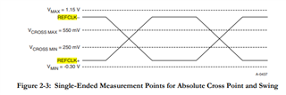
The table in datasheet does not specify DC common mode voltage range that is acceptable/recommended. The table labels the spec VRX-CM-DC = DC(avg) of |VREFCLK+VREFCLK-|/2, but doesn’t include an acceptable level. Our customer's current DC couple implementation has a common mode voltage at around 0.84V. Is this within the recommended level? What is the spec limit?

2) In the datasheet it states that the REFCLK+, REFCLK-, RXP, and RXN do not need external components and thus can be DC coupled rather than AC coupled (ie does not need in-line caps). Is it problematic if these lines were AC coupled exactly like the TXP and TXN lines?

3) Is the REFCLK expected to have a common source between the PCIe link partners (i.e. same oscillator is used to generate REFCLK for both the PCIe switch and the End-Point (DDC PCIe bridge) ? 

I see in the datasheet that it says the XIO2001 supports a local generated clock so my first thought is that it is fine not to have the same common source. Correct?

4) When our customer shuts down their board and thus removes the 3.3V from the rail of the XIO2001, a voltage of about 1.6V can be seen on the 3.3V rail of XIO2001. I read in one of the forums that there are power modes such as L2 that cause the XIO2001 to back feed from Aux voltage on to the 3.3V rail. Is this true or did I miss understand this? Our customer has not yet ruled out the cause being something in there system. However, due to the vast number of I/O in there system we are trying to understand where best to look for the cause of this voltage and therefore any information about known issues, signals, or modes that would cause back feeding of the device to the 3.3V rail would be very helpful in directing us where to look first. BTW, at room temp the 1.6V is present on the XIO2001 rails and the device powers up and establishes a link (L0 state) just fine. However, at -40C (after a soak) it does not.

5) When the datasheet states the XIO2001 is rated for -40C, is that case temperature (ie touch temperature of the BGA case rather than internal die temperature achieved by an extended cold soak)?

  • Hi David:

      Is this new design? At what temperature XIo2001 start fail?

    1) What is the common mode voltage on receiver clock input pins (RXP, RXN)?

    since TXP/TXN from other side is AC coupled, so RXP/RXN common mode voltage should be around 0V.

    2) In the datasheet it states that the REFCLK+, REFCLK-, RXP, and RXN do not need external components and thus can be DC coupled rather than AC coupled (ie does not need in-line caps). Is it problematic if these lines were AC coupled exactly like the TXP and TXN lines?

    REFCLK is DC coupled for PCIe spec, so no AC cap needed for REF clk.

    For RXP/RXN , you can add 330nf cap or no cap since TX side is AC coupled.

    3) Is the REFCLK expected to have a common source between the PCIe link partners (i.e. same oscillator is used to generate REFCLK for both the PCIe switch and the End-Point (DDC PCIe bridge) ? 

    yes,PCIe link partners should genete REFCLK with DC common mode max common  mode voltage is  0.55V

  • I would like to amend this and ONLY concentrate on the REFCLK+ and RECLK- since it was discovered to be the source of our customer's issue. Therefore, ignore everything else for now other than what is below.

    Is there a DC common mode voltage range spec for REFCLK+ and REFCLK- when the XIO2001 is configured to use a synchronous 100MHz Differential Clock?

    Would a common mode of 0.84V be an issue for the XIO2001?

    PCIe spec calls for a Vcross of 250 to 500mV. I do not see this in the XIO2001 datasheet. Is it required to meet this Vcross for the XIO2001 to operate correctly? What would be the ramifications if we did not meet this? Is there a certain amount of known margin that we can violate this by?

    When operating in the 100HMz Synchronous Ref Clock mode, is it expected to use a common source between PCIe link partners (ie same oscillator is used to generate the REFCLK for both PCIe switch and End-Point)? Will the XIO2001 work if a common source clock were not used? What would be the known ramifications is we did not use a common source clock but still used and configured the bridge for a 100MHz Differetial CLock.

  • 4) When our customer shuts down their board and thus removes the 3.3V from the rail of the XIO2001, a voltage of about 1.6V can be seen on the 3.3V rail of XIO2001. I read in one of the forums that there are power modes such as L2 that cause the XIO2001 to back feed from Aux voltage on to the 3.3V rail. Is this true or did I miss understand this? Our customer has not yet ruled out the cause being something in there system. However, due to the vast number of I/O in there system we are trying to understand where best to look for the cause of this voltage and therefore any information about known issues, signals, or modes that would cause back feeding of the device to the 3.3V rail would be very helpful in directing us where to look first. BTW, at room temp the 1.6V is present on the XIO2001 rails and the device powers up and establishes a link (L0 state) just fine. However, at -40C (after a soak) it does not.

    looks like if there are too many caps on supply which cause it discharge too slow, you will see voltage still on main power supply.-40C is case tempertaure

    5) When the datasheet states the XIO2001 is rated for -40C, is that case temperature (ie touch temperature of the BGA case rather than internal die temperature achieved by an extended cold soak)?

    -40C is case temperature.

    Best

    Brian

  • The XIO2001 starts to fail between -21C and -40C in the customer's system. In other words it does not start to work until temperature is greater than -21C. This is a new customer program.

  • You say PCIe link partners "should" have a common source REFCLK. I realize that its is a typical and recommended clock scheme for PCIe in general. However, is that a recommendation or specific requirement for use of the 100MHz REFCLK for the XIO2001? 

    Every where I look this up uses words like "recommended" or "typical clock scheme" but never actually states "required to be".

    Our device has the the 125MHz Asynchronous single-ended reference clock option disabled with the intention of only allowing the system clock design approach using a differential 100MHz REFCLK. Our understanding and expectation, based on the TI datasheet, would be a common source REFCLK between all PCIe partners would be required since to use a local clock (ie Oscillator locally just for a single PCIe end-point device) would require using the 125MHz single-ended clock. Hence the reason there are two options in the XIO2001 in the first place. Correct?

    Just from the XIO2001 point of view, can the 100MHz REFCLK be used as a differential asynchronous reference clock thus allowing different clock source for the PCIe end-point devices than the actual PCIe switch and Root Complex?

    If someone were to do this, what do you think the ramifications or issues with the XIO2001 would be?

    For example, assume a single ended local oscillator on a board that feeds a clock generator chip that produces the 100MHz Differential REFCLK on that board only for the two PCIe end-point devices on that board. However, the root complex and any PCIe switch tied to the root hub are on a different board which run on a differential clock produced on that board using identical parts as the first board. The RXP, RXN, TXP, TXN, etc for the two PCIe end-points leave their board via a connector and go to appropriate switch and/or root complex. Other than the obvious timing issues that this is likely to cause which would result in an increase in BER especially once large amounts of data starts to be transferred, would this scheme have any other known negative impact on the XIO2001 device itself for lets say things like establishing a link and getting to L0 state. We are trying to figure out how much the use of a clock scheme like this is contributing to the failure to establish a link at -40C, even though at temperatures warmer than -21C there is no issues with establishing the link.

  • reason there are two options in the XIO2001 in the first place. Correct?

    This is correct.

    So what is the issue? XIO2001 not detected or the PCI device not detected?

  • for clock architectures:

    the Common Clock is the most widely supported clocking method used by commercially available devices. An advantage of this clocking architecture is that it supports spread spectrum clocking (SSC) which can be very useful in reducing electromagnetic interference (EMI) with less stringent reference clock requirements than SRIS. A disadvantage is that the same clock source must be distributed to every PCIe device while keeping the clock-to-clock skew to less than 12 ns between devices..

    for Separate Reference architectures.

       it don't have skew issue, but maybe adding more jitter source.

    Here is the document talking about  PCIe clock  architectures:

    PCIe-Clock-Source-Selection.pdf

    Best

    Brian