Part Number: DP83869HM
Tool/software:
Hi,
I am trying to prepare FPGA timing constraints in order to connect to DP83869HM PHY via RGMII interface. I am confused about the timing tables and diagrams provided in the datasheet. Therefore, I would like to ask your support for clarification.
I would like you to confirm my understanding is correct as below:
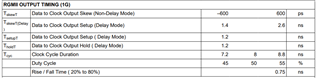
- Section 6.6: OUTPUT TIMING table corresponds to TX signals from PHY to FPGA.
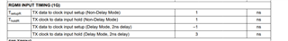
- Section 6.6: RGMII INPUT TIMING table corresponds to RX signals from FPGA to PHY.
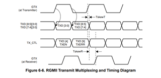
- Section 6.7: Figure 6-6. RGMII Transmit Multiplexing and Timing Diagram corresponds to TX signals from PHY to FPGA.
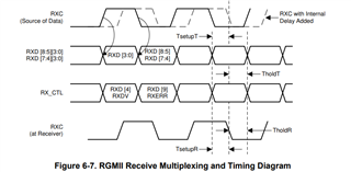
- Section 6.7: Figure 6-7. RGMII Receive Multiplexing and Timing Diagram corresponds to RX signals from FPGA to PHY.
Thanks in advance,