Part Number: TIOL221
Tool/software:
Hello!
We are using TIOL221 in pin mode and have encountered several issues that need to be confirmed. Please clarify them. Thank you.
1. We need to keep EN1 and EN2 in both high/low states. Can their pins be directly connected together to save wiring space? Supply 5V voltage to it through a 5k Ω pull-up resistor (when separated, 10k Ω should be used separately, equivalent to two resistors of the same specification connected in parallel) to ensure that it remains in a high level state?
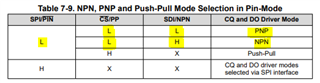
2. As mentioned above, can the CS/PP and SPI/PIN pins be directly connected together? Connect a 5k Ω pull-down resistor (when separated, 10k Ω should be used separately, which is equivalent to two resistors of the same specification in parallel) to ground and keep it in a low level state?
3. When using the pin mode of TIOL221, some pins (RX1, V5IN, DI, RESET, RX2, WU, SDO/NFLT2, SCK) do not need to be used. Do we need to connect these pins through pull-up/pull-down resistors?
4. Is it appropriate to connect the VOUT pin of TIOL221 to ground through a 1uf capacitor?
5. The INT/NFLT1 pin outputs a high level during normal operation and a low level during output faults. So when the output is high, should it maintain a constant voltage source min (VOUT+0.3V, 6V) output, or a constant current source (-5mA, 5mA) output? Or is there a specific relationship between the output voltage and current of this pin? Furthermore, can the INT/NFLT1 pin be used as an analog output? If it is connected to the VOUT pin through a 10k Ω pull-up resistor, will the high resistance state of the pin be converted to a 5.3V voltage source output?
At the same time, the output current range of the INT/NFT L1 pin (-5mA, 5mA) means that the maximum current allowed to flow through it is 5mA, including the maximum current allowed to flow through it. That is, the maximum current allowed to flow from VOUT to the INT/NFT L1 pin is 5mA?