Tool/software:
Hi,
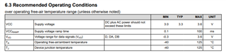
As the TMUXHS221 is 5V tolerant on Data Pins (abs max. 5.5V), it is our selection for switching two USB 2.0 connectors to the CPU.
As the block diagram shows a charge pump for the analog switches, I assume signals above 3.6V are just forwarded and not clipped by the switch, or is there any clipping of signals between 3.6V and 5.5V expected due to the voltage level of the internal charge pump?
Our CPU has abs max. the voltage on data pins is 3.73V. If the MUX is limiting the voltage on the Data lines from DA/DB to D to max. 3.73 we can skip the protection between the MUX and CPU.
Can you please tell me the transfer behavior between 3.6V and 5.5V on the Data pins in Direction DA -> D and DB-> D?
Many thanks and best regards.
Olli