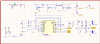
Part Number: TCAN2451-Q1
Tool/software:
1. Please review the schematic design of TCAN2451-Q1 for our BMS design.
2. The output voltages are VCC1 = 3.3V and VCC2 = 5V. Could you to confirm that, whether the SPI output levels will be 3.3V as per VCC1 or 5V?
3. As per the datasheet, nINT pin is active low, so this pin has to be pulled up or not with 3.3V (VCC1)?
4. What is the functionality of SW pin?