This thread has been locked.

If you have a related question, please click the "Ask a related question" button in the top right corner. The newly created question will be automatically linked to this question.

TDP0604: Use of TDP0604 or SN65DP159 without DDC (DP++ to DVI application)

Part Number: TDP0604
Other Parts Discussed in Thread: SN65DP159, DP159RGZEVM,

Tool/software:

Hello TI

Our application uses an Intel processor on a COMe computer board.

We are using the DDI for monitor output. The datasheet for the computer module specifies DDI is DP++ capable.

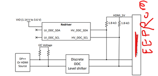
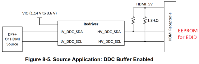
We want to output video to an external DVI monitor.

However, the external monitor does not support the DDC interface, but has fixed known resolution.

Can the TDP0604 or SN65DP159 be used in this case? Is the DDC interface required?

Also, how should we couple the in- and outputs with respect to AC and DC? 

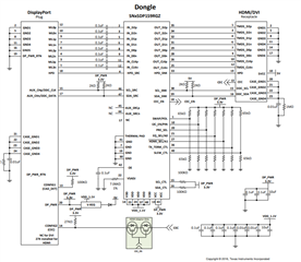
We currently have an implementation using the TDP0604 with AC coupled inputs and DC coupled outputs, this setup is currently not working.

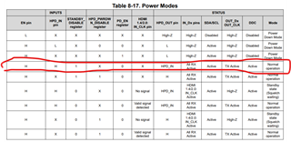
We intend to use the TDP0604 in strap mode.

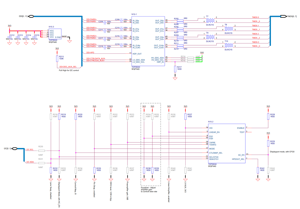
We have attempted to add a pull up resistor to 5V on HPD_IN with no success.

Can you please help us get closer to a solution?

Regards

Lars

  • Lars

    You can use TDP0604 and DP159 without DDC, but both the source and TDP0604/DP159 have to be manually configured to support the particular resolution.

    Looking at the schematic, below are my comments:

    1. Remove R228 and add a 0.22uF pulldown capacitor

    2. Remove R229 and populate R243

    3. Populate R240

    4. Need to tune R238 and R239 depends on the output signal quality

    5. Remove R219 and populate R233

    6. Leave both LV and HV DDC floating since you are not using DDC

    7. Pull HPD_IN to 5V

    If you probe the TDP0604 clock output, do you see a clock output? And does that clock output frequency match with the targeted resolution?

    Thanks

    David

  • Thank you for your reply David.

    With respect to your points:

    1) Removing R228 would never enable the device, so this cannot be right? Section 9.2.1 of the datasheet specifies a 100nF cap to GND, we have tried to add this to our PCB as well.

    2) Pulling AC_EN down will make the TDP0604 be DC coupled. How is this a good idea when the display source is DP++?

    3) Pulling LINEAR_EN low is recommended for source application as per table 8-4 so I see the point in doing this.

    4) We can tune these when we get video through. It is more related to optimization, currently we get no video through.

    5) Pulling GFG0 low together with AC_EN low, as suggested in your point 2, makes HDMI termination open per table 8-13. What is the point of this?

    6) Understood

    7) Is this required for the TDP0604 or the display source?

    Currently we do not see any activity on the clock output. We are also in communication with the manufacturer of the COMe module, as the module may require a response on the DDC lines to start video transmission.

    We are also investigating if adding an EEPROM on our PCB and connecting the DDC lines of the TDP0604 (on the HV side) could be a solution. This EEPROM would then need to be placed on I2C address 0X50 and contain EDID (with our prefered display resolution) for the COMe to read. This will basically simulate an external monitor.  Do you think this is a better solution than not connecting the DDC lines?

    Regards

    Lars

  • Hi Lars,

    Please see my response below

    1) The TDP0604 EN pin has a internal 250k pull-up to VIO, so you don't need the external pull-up resistor. Along with the external pulldown capacitor, this creates a passive reset circuit and capacitance can be changed to decrease/increase the reset timing depending on the VCC power ramp up time.

    2) The TDP0604 input can support both DC and AC coupled input without any control. The AC_EN pin controls the DC or the AC coupling of the TDP0604 output, so in this case, we want to set AC_EN pin low since TDP0604 output is DC coupled.

    5) Pulling CFG0 and AC_EN both low will change the termination depending on the pixel clock frequency. But termination will impact the signal quality, it will not impact the issue of video not going through.

     7) Please see the table below for the TDP0604 Power Modes. When EN is high, it is important that HPD_IN needs to be driven high as well for the TDP0604 to be in normal operation mode. Otherwise TDP0604 will be in power down mode with all outputs in Hi-Z state.

    Please also note that the HDMI TMDS is a current mode driver. When you are measuring the CLK output and with the output being DC coupled, you need to connect the output to a 50ohm termination network to 3.3V in order to see a signal. 

    If the COMe module does require a read of DDC lines to start the video, then you can use an external EEPROM and I don't see an issue with your proposed implementation. You can implement the EEPROM as shown in below block diagram. The DDC buffer must be enabled and the LV DDC pins must be floating. This connection is supported in pin-strap mode when MODE pin is "0" or "1". In I2C mode, the DDCBUF_EN register must be set to enable the DDC Buffer.

    Thanks

    David

  • Responses below:

    1) understood, we will not mount the external PU resistor and only mount the capacitor to GND

    2) OK, since we want DVI, we have DC coupled the output, I agree AC_EN must be tied low. Must we add the 50Ohm resistor to the final application or is that only required when no display is connected?

    5) When we get video through, we can optimize the termination according to table 8-9.

    7) Understood, We will ensure that both EN is high and HPD_IN are high. Are there any requirements relating to the sequence? For instance, must EN be high prior to HPD_IN changing to high or is the sequence irrelevant for correct operation?

    With respect to the EEPROM, could we use the configuration in Figre 8-5 of the datasheet? This will save us the external level translator.


    The implementation will then look something like this:

    We then expect to close the connections in X14 on the HV side to the EEPROM. Will this be a feasable solution?

  • We are also attempting to implement the SN65DP159 for the same solution. Can you please comment on this implementation?

    The schematics are attached here.

  • By the way, dont mind the EDP signal naming. The video source is the DDI interface on the COMe module for the retimer as well.

  • Lars

    Please see my response below.

    2) OK, since we want DVI, we have DC coupled the output, I agree AC_EN must be tied low. Must we add the 50Ohm resistor to the final application or is that only required when no display is connected?

    The 50ohm to 3.3V termination is only for measuring the TDP0604 DC coupled output since the scope normally does not provide 50ohm termination to 3.3V. Most DVI monitor should internally have the 50ohm to 3.3V termination in their RX so external 50ohm is not required. 

    7) Understood, We will ensure that both EN is high and HPD_IN are high. Are there any requirements relating to the sequence? For instance, must EN be high prior to HPD_IN changing to high or is the sequence irrelevant for correct operation?

    There is no timing requirement between the EN and HPD.

    With respect to the EEPROM, could we use the configuration in Figre 8-5 of the datasheet? This will save us the external level translator.

    I do not see an issue with your proposed implementation. For the TDP0604 LV_DDC, it has internal pullup, so no external pullup is required. If you are snooping on the LV instead HV side, please disable the TDP0604 DDC buffer.

    On the DP159, I would not connect EEPROM on the SDA_SRC and SCL_SRC. Please note DP159 DDC supports clock stretching, so the DP++ source has to support clock stretching as well.

    Thanks

    David

  • I am glad you do not see an issue with this implementation. The internal pull ups on LV DDC pins are evident from section 8.2 in the data sheet. We will not mount external pull up resistors. If we choose this implementation, the snooping is done internally to the TDP0604 and no configuration is required, correct? This is stated in section 8.4.1.

    An additional question: From table 8-17, it seems that row 5 is a power mode where the device does not power down but keeps both RX and TX active at all times. Is this correct? It seems that HPD_IN is don’t care in this situation (I guess the registers must be written over I2C in this case.

    With respect to the retimer, we will not use EEPROM on the source side, but EEPROM with EDID on the Sink side. The COMe module suppers DP 1.2 ++ and both DDC over I2C or a differential AUX channel for configuration. As long as we just pick either one (not simultaneously), both should work equally well, correct? Is clock stretching still an issue if using the differential AUX interface?

  • Hi Lars,

    If we choose this implementation, the snooping is done internally to the TDP0604 and no configuration is required, correct? This is stated in section 8.4.1.

    Yes, and the DDC buffer must be enabled with MODE pin is "0" or "1". 

    it seems that row 5 is a power mode where the device does not power down but keeps both RX and TX active at all times. Is this correct? It seems that HPD_IN is don’t care in this situation (I guess the registers must be written over I2C in this case.

    Yes, this is using I2C register to ignore HPD pin (never goes into Low Power mode) and also disable the Standby mode when there is no input signal being present at IN_D2 or IN_CLK. So basically it forces TDP0604 into the always active state with PD_EN bit = H. 

    The COMe module suppers DP 1.2 ++ and both DDC over I2C or a differential AUX channel for configuration. As long as we just pick either one (not simultaneously), both should work equally well, correct? Is clock stretching still an issue if using the differential AUX interface?

    Please see below for the DDC/AUX implementation for this particular case. In this case, you are still using DDC which supports clock stretching, and DP159 AUXP/N are left un-connected.

    Thanks

    David

  • Thank you for that explanation.

    But please could you respond to my question in the previous post? Is clock stretching an issue if I2C-over-AUX is used? The DP++ source on the COMe module we are using has a configuration pin on the module to select either single ended I2C or differential AUX from the source with respect to DDC.

    But it seems both redriver and retimer IC may be a solution for us. We have already sourced the TDP0604EVM and I will source the DP159RGZEVM as well for some testing. We have a carrier board for the COMe module from the manufacturer with DP output (only series capacitors on the carrierboard) to a DP connector. This could be connected directly to the DP159EVM and we could then use a passive HDMI adapter to DVI. This would enable us to do some quick testing.

    We actually don’t need to support high resolution, the max resolution will be 720p (1280x720). Is it a viable solution then to write a 1 to DDC_TRAIN_SET register as specified in section 9.5.4.2.3 of the SN65DP159 datasheet? This should disable the DDC training. Should we leave the SCL and SDA pins floating on both source and sink side for this configuration? We will never need HDMI 2.0 support, only DVI 720p resolution max, or lower such as 307k (640x480).

  • Hi Lars,

    I2C-over-AUX does not support clock stretching if you are using it. 

    You can leave DDC_TRAIN_SET either '0' or '1'. If '1', then DP159 can only working in HDMI1.4 or DVI mode. If '0', then DP159 can also support HDMI2.0 depends on the DDC snooping. 

    If you are not using DDC snooping, then tie SDA/SCL_SRC to GND, and tie the SDA/SCL_SNK high through 4.7k resistors.

    Thanks

    David

  • Thank you for your response. We have now successfully implemented the TDP0604 and we have display output on a monitor without DDC. We are are also investigating the DP159 and we have made an implementation of this IC on a PCB. We have the following implementation:

    COMe module DDI interface is connected to DP159. The 4 high speed pairs are AC coupled. HPD from COMe is connected to HPD_SNK. DDI SDA on COMe is connected to DP159 SDA_SNK and DDI SCL on COMe is connected to DP159 SCL_SNK (both with 2K PU to 3V3).

    With respect to DP159 configuration, we have all config pins left floating except HDMI/DVI select is pulled up with 65k to 3V3 for DVI mode and I2CEN pin is pulled down with 65k for pin strap mode. VDD pins are verified to be 1V1. VCC pins are verified to be 3V3. OE is verified to be sufficiently delayed (with an external capacitor) relative to 3V3 voltage rise. HPD_SRC is verified to be 5V. HPD_SNK is verified to be 3V3. We have probed SDA_SRC and SCL_SRC for I2C communication and we have verified both request from COMe and reply from monitor (the 128 bytes on I2C address 0x50 in the monitor). We have probed the high speed input lines and we see dato on these lines (all 4 pairs). However, we see no output on the TMDS outputs (none of the 4 pairs). How can this be? Since both HPD and DDC SCL and SDA are translated correctly the IC seems to be in operating mode. We have attempted to force the IC in reset by forcing OE to GND potential and this reduces the current consumption on 3V3 so the IC is drawing power). Can you please suggest steps for us to move for?

    Regards Lars

  • Lars

    Can you please share your latest DP159 schematic?

    When probing the DP159 output, did you provide external 50ohm termination 3.3V in the scope? The TMDS/DVI is a CML output and expects to see 50ohm termination to 3.3V in order to generate the proper output.

    Thanks

    David

  • Yes, the schematic is attached.

    DVI Test Board for TI.pdf

    Please note, that the EEPROMs can be connected and disconnected from the circuits using the jumpers.

    Currently, we have all jumpers disconnected. The DDC info is read from a standard monitor from the DVI connector.

    We do not have any terminations on-board, but I am thinking that a standard monitor with a DVI input have the terminations internally?

  • Lars,

    The DVI monitor should have internal 50ohm termination to 3.3V, so you could connect a DVI monitor to the DP159 output and then use a high impedance active probe to probe the DP159 output. I would look at the clock first and make sure the clock frequency matches with your targeted DVI resolution pixel clock frequency. 

    Please also check the COMe Module DDI interface lane order and make sure the lane order followed the DP++ spec as shown below.

    Thanks

    David

  • I have just checked and I can verify that the COMe DDI lane order is according to the spec (e.g. DDI lane 0 + corresponds to ML Lane 0 (p)). In the design, DDI lane 0 is connected to TMDS lane 2, DDI lane 1 is connected to TMDS lane 1 and DDI lane 2 is connected to TMDS lane 0. DDI lane 3 is connected to TMDS clock. This seems OK from my point of view. Please note that the TDP0604 implementation on this board is functioning correctly. Since I am using the same implementation for the DVI connector, I am confident that the connections to the connector are correct for the DP159. Are we in agreement that the DP159 should output video in this case?

    For reference, we have attempted a similar electrical setup using evaluation boards, specifically a COMe carrier board connected to the DP159RGZEVM. The actual COMe module we are using is the same in my own implementation and in the carrier board (which also means that all SW is the same). The COMe carrier board features 100nF series capacitors on the DDI lanes before being routed into a DP connector. The AUX+ and AUX- are routed into the DP connector directly (for DDC CLK and DDC data), the same for HPD. The CAD (pin 13) has a PD of 1 Megaohm on the carrier, but this is "overwritten" on the DP159EVM which has a 100kOhm PU to 3V3. We connect the DP cable to the DP159EVM DP input connector. The EVM is the configured in the exact same way as our own PCBA. We then connector an HDMI cable to the HDMI output connector which in turn is then connectoed to a passive HDMI to DVI adaptor. This adaptor is then connected to the same external monitor. This setup shows output video without any issue. I fail to see how our implementation is different to the evaluation setup, which is why I am asking you for help to figure out what to do next.

    Can you identify anything wrong with my own implementation?

  • Lars

    Can we please do a experiment by putting DP159 into the I2C mode, and change its operating mode into redriver mode only? Please write the last two bits of register 0x0A to 0x00 for the redriver mode. 

    Thanks

    David