This thread has been locked.

If you have a related question, please click the "Ask a related question" button in the top right corner. The newly created question will be automatically linked to this question.

UCC24624: Increased FET loss due to early turn-off

Guru 12155 points
Part Number: UCC24624

Tool/software:

Hi,

We are currently using the UCC24624 in an LLC resonant converter and are facing a problem where the SR MOSFET gate turns OFF before the drain current reaches zero. This results in extended body diode conduction, leading to increased power loss and heating.

As shown in the attached waveform (highlighted in red), significant drain current remains at the time of gate turn-off.

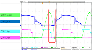
Based on the datasheet, we suspect this is due to the fixed VTHVGOFF = 10.5 mV turn-off threshold.
We have already implemented the recommended resistor between the VSS pin and the MOSFET source to increase the turn-off threshold, but did not observe significant improvement.

We would appreciate your guidance on the following points:

  1. Is such early turn-off behavior commonly attributed to parasitic inductance or MOSFET package-related effects?

  2. Are there any additional countermeasures beyond adjusting the VSS threshold that may be more effective?

  3. Do you have any recommendations regarding PCB layout (e.g., routing of VD/VSS or PGND) to help mitigate this issue?

Thank you very much for your support.

Conor

  • Hi Support Team,

    Is there any update?

    Best regards,
    Conor

  • Conor,

    Are you observing this behavior across all operating conditions or only on a specific condition?

    Please also share the schematic with us.

    Best,

  • Hello Conor-san, 

    As Ning requests, please provide a schematic diagram of the SR circuit.  Be sure that the resolution of the image is high enough for the component values to be readable.

    For your 3 questions: 
    1.  Early turn-off is commonly attributed to stray inductance is both the pcb layout and in the MOSFET leads.  Lead inductance is the typical package-related effect.
    2.  The most effective countermeasure beyond adjusting the VSS threshold is to minimize or eliminate the stray inductance.  This involves careful pcb layout and choosing MOSFETs with minimal leads. 
    3.  The datasheet has layout guidelines listed in Section 11.1 on page 27.  Ironically, the layout example Figure 11-1 does not strictly follow all of the listed guidelines in Section 11-1.  In my opinion, I think the example figure could be much better than it is.  Specifically, the VSS pin should not be tied to PGND through the via as shown, but should be connected directly back to the source pins of the MOSFETs as stated in the 4th bullet in the list. 

    Since the peak current in your waveform is 29A, I presume that you may be using large MOSFETs with longer leads (such as TO-220 or TO-247 packages).
    Such leads can have several nH of inductance.  Making a rough estimate of di/dt, I see ~12.5A/800ns = 15.6mV/nH.  

    The proportionable gate-drive is engaged just after the current peak of 29A which is expected, but shuts off around 25A where the di/dt starts to become high.  This indicates that inductance generates most of the VDx-VSS voltage that is being sensed by the controller. 

    Please examine the pcb layout and revise as necessary to eliminate any inductance in the Vds sense path.  If at all possible, choose leadless MOSFET packages.  If not possible, do the best that you can with a VSS offset resistor as discussed in Section 8.3.3.  

    Regards,
    Ulrich