This thread has been locked.

If you have a related question, please click the "Ask a related question" button in the top right corner. The newly created question will be automatically linked to this question.

DS90LV011AQ-Q1: eye diagram

Part Number: DS90LV011AQ-Q1

Tool/software:

team,

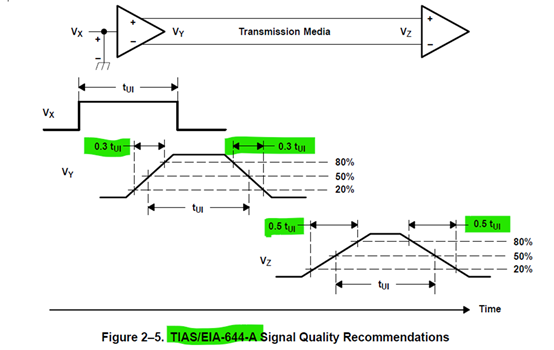
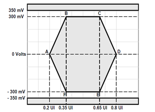
Would we have the eye diagram for the 011 and 012 at 20Mbps or guidance on what eye diagram limits we should expect in order to validate ? similar to below:

thanks

  • Hi O'Mellin,

    No we don't have a specific eye diagram for this device to share.  Any part that starts with DS came from National and they had horrendous record keeping more often than not (i.e. very little documentation) 

    However as far as guidance goes on the eye mask - they can derive it from the datasheets and I will quickly go over how to do that. 

    The max and min levels (represented by the grayed out bars at the top and bottom of the given chart) should be abs max ratings - or since this differential the maximum output of the diff driver with a standard load (100 ohms) - that is going to be +/-450mV - so instead of +/-350mV like shown in reference it should be +/-450mV. 

    The Y-Axis position of points B, C, F, and E should be based on receiver thresholds (basically anything lower than F or E will definitely give a logic 0 and anything higher than points B or C will give a logic 1). 

    For the 012 that would put B and C Y-Axis position at 0V and F/E at -100mV. Anything at -100mV or lower is a logic low and anything that is 0V or higher is guaranteed to be a logic high. 

    A/D should just be the halfway points between them - so -50mV would be a good place to put it. 

    The X-axis positions would be the same on this guidance - we don't want transition times to take up more than 1/3 of the total interval - the x-axis distance from A to F and E to D is 0.15UI - and when you add both of them up that gives you roughly 1/3 of the time dedicated to transition time. Replace 1UI as 1/(10MHz) = 100ns (assuming double data rate - i.e. one cycle transmits 2 bits - if it is one cycle per one bit then it would be 50ns). 

    The thresholds on the receiver device are not symmetric across zero so the eye mask doesn't need to be symmetrical either - however the eye opening most likely will be symmetrical because the driver has the same drive strength regardless if it driving high or low - the offset is so that the bus will read idle voltages as a logic high. 

    This is a pretty quick/crude eye diagram mask - but it should capture all the needed elements to test SI with these devices. 

    So in conclusion. 

    Grayed out bars should be place >450mV and <-450mV as you shouldn't have differential voltages larger than that. 

    A should be placed at [-50mV, 0.2UI]

    B should be placed at [0V, 0.35UI]

    C should be placed at [0V, 0.65UI]

    D should be placed at [-50mV, 0.8UI]

    E should be placed at [-100mV, 0.65UI]

    F should be placed at [-100mV, 0.35UI]. 

    If the eye opening passes that mask test - you should have good data integrity. 

    Please let me know if you have any more questions!

    Best,

    Parker Dodson

  • Hi Parker, 

    I am following up on this thread as Olivier is OoO. Could you please share the acceptable limits of the following parameters:

    1) Rise & Fall times of LVDS at the transmitter end + Receiver end.

    For example: 

    2) Bit error rate

    3) Pk-Pk jitter

    4) Mask hits (Violations at mask)

    5) If any...

    Please share any reference application note (TIA/EIA-644-A Standard) on signal quality.

    The customer is also looking to have a meeting with one of our expert to discuss this, I will contact you by email.

    Thanks !

    Geraldine

  • Hi Geraldine,

    Sorry for the delay while E2E was down for maintenance. 

    1. Figure 2-5 that you share are the LVDS recommended values.  So at driver end 0.3 * unit interval and 0.5 * unit interval at the receiver. 

    2. It is going to depend on the needs for the application itself - the LVDS bus does not care about the bit error rate - but on other devices we have been able to achieve a BER of 1 x 10^-12 - note here: https://www.ti.com/lit/an/snla154/snla154.pdf?ts=1752508339235&ref_url=https%253A%252F%252Fwww.google.com%252F - while not 1:1 it can show that you can get your bit error very low - and you should aim for as low as possible. 

    3. pk to pk jitter is similar to BER - it will depend on the end application needs - the LVDS bus will operate with/without jitter. in general there are two guidelines we would suggest when determining jitter. First the sum of all the jitter components in the system (transmitter, media, receiver) should be less than 1 bit time. Second the jitter should be less than 20% of the unit interval (or lower - typically 5% to 20% is the general range - but lower is better). However - the end application is going to dictate more precise values. For example - for clock distribution we see tens of ps (like 50ps) jitter reqs - but that is end equipment system dependent. 

    4. This is going to be similar to BER - you ideally want none - but it is going to be system dependent on what the actual mask violation limit will be. 

    Really I don't have much else to add - the main concern is going to need to be spec'ing this correctly for their specific system - this isn't something you can do with the device alone - you need to consider the entire communication pathway including devices and layout. 

    Please let me know if there are any more questions and I will see what I can do - we should be connected on email if a meeting is still needed. 

    Best,

    Parker Dodson