A related question is a question created from another question. When the related question is created, it will be automatically linked to the original question.
If you have a related question, please click the "Ask a related question" button in the top right corner. The newly created question will be automatically linked to this question.
You will not be able to switch the LEDs off; when you try to configure the pins as high, current will flow through the clamping diodes into VCC. And when no other device is able to sink that current, VCC will rise and destroy all devices connected to it.
Use a high-voltage driver like the TPL7407LA, or an integrated I²C LED driver like the TPIC2810.
P0 looks to be okay since this is a general reset pin.
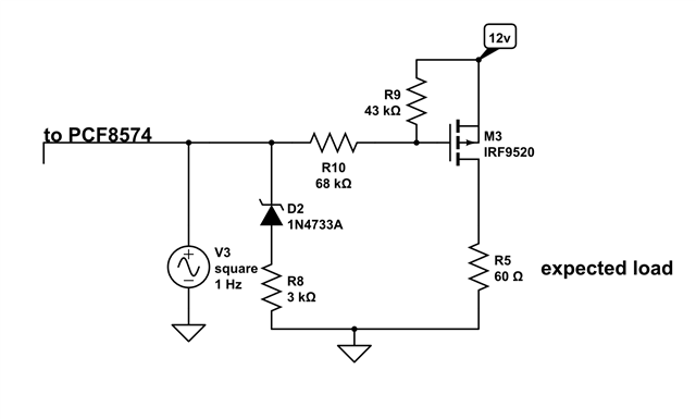
P4 - P7 look okay in this case. The 2N7000 is being used as a switch to sink current through the LED from the 12V supply. I don't see any issue with the 12 V supply interfering with the Px pin.
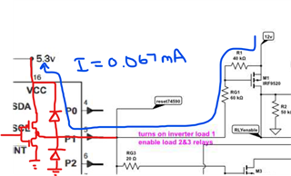
My concern is with P1 - P3. I have not seen the PCF8574 used with driving an inductive coil. I have my concern with the 12V supply and R1 and RG1. IF I assume little current goes into the gate of M1, then 12V forms a resistive divider across 40k and 60k resistors. There is a positive facing diode on the I/O pin that would back feed into the 5.3 V power supply :
Not sure if this would work for your use case, but there would be current flow in the high state.
Also, since IRF9520 is a p-channel FET, wouldn't this mean that the gate-source voltage is always greater than the threshold?
5.3 V - 12 V = -6.7 V
0 V - 12 V = -12 V
So whether P1 is driving HIGH or driving LOW, the FET at M1 would always be ON.
I don't think this solution will work since PCF8574 is not a 12V device.
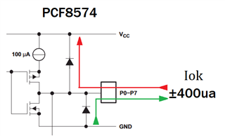
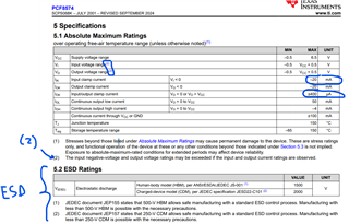
Tyler, I am not trying to be contrary, i just want to be sure I have a proper outcome. There are some subtleties involved that may be explained below. FROM: Understanding and Interpreting Standard-Logic Data Sheets Application Report - SZZA036C – December 2002 – Revised June 2016 4.4.7 Output Clamp Current, IOK This is the maximum current that can flow safely into an output terminal of the device at voltages above or below the normal operating range. Helpful Hint: If there are clamp diodes between the device outputs and the VCC supply (see Figure 28), for ESD protection or parasitic current paths in the output P-channel pullup transistor, there will be both a positive and a negative absolute-maximum rating for the output clamp current. If there is only a negative absolute- maximum rating, that implies that there is only a ground-clamp diode at the output, not a power-clamp diode or a parasitic current path in the output P-channel pullup transistor.
FROM: APCF8574 datasheet IOK Input/output clamp current VO < 0 or VO > VCC ±400 μa I have done my best to analyze the circuit using "Circuit Lab" (https://www.circuitlab.com). The schematic is listed as public and is tagged withe both IRF9520 or PCF8574. Based on the results below, the IOK would be ≈ 67ua - under the 400ua limit. The turn on/off gate voltages appear to be appropriate. I hope this is helpful. Let me know if I am in left field. Thanks Barry
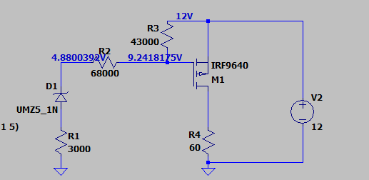
The MBR diode might not best represent the characteristics of the diode inside the PCF device as this has ~ 300 mV forward voltage, the diode inside the PCF8574 is likely 0.5V.
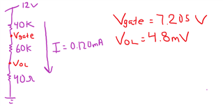
IF the voltage at P2 is 5.3V + 0.5V = 5.8V, then the current from V1 to P2 is (12V - 5.8V) / 100k = 62 uA.
Vgate = 5.8V + (62 uA x 60 kohm) = 9.52 V
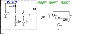
A Vgate = 8.5V or greater seems to turn off M1. So for case where SW1-3 is open or SW2 is closed, LOADV = 0V which means M1 is off.
FOr SW3 closed case, SW3 is modeling the nFET of the output driver. There is some resistance there that would create a voltage drop.
If we look at the IOL / VOL specs of the PCF8574, then the impedance of the pull-down driver is roughly 1V / 25 mA = 40 ohm.
I calculated the voltage drops using the driver specs.
Looking at the specs for IRF9520 Vgs:
-4.0V is the recommended max. 12- 4 = 8V, so technically Vgate should be >= 8.0V. THe abs max conditions for this power FET look to be +/-20V, so technically we are still in spec here.
My calculation of Vgate = 7.205 V will be okay, and the M1 will turn ON and LOADV = ~ 12V.
You are correct that PCF8574 has abs. max of 400 uA current limitation on the clamping diode. Since 67 uA is the calculated current, I suspect that this application is okay even though there is current back feeding into the supply. As long as this current works in your system, then I think you can use the PCF8574 device in this situation.
Tyler, I need to ask for your help again. I have no idea if you can help. I posted the following on the Arduino Forum. forum.arduino.cc/.../1393532
My interpretation of Iok is the maximum allowable current through the clamping diodes. 70ua is less than that (15% of the max) should be a safe operating condition. If you disagree, please share your interpretation of Iok. Surely, Iok is not a useless parameter
Unfortunately, I received significant negative feedback concerning what "Iok" means. I feel very comfortable in your assessment. However, this is some of the feedback I received.
"The TI forum is just like this forum. You might find someone who is knowledgeable or someone who is just guessing.Obviously this Tyler person has not read the datasheet."
"Those diodes are there for transient ESD protection only. They should not be used for clipping or clamping input signals. Operation with continuous current through the diodes is unspecified."
"After you have done a few designs, you will come to realize that these tricky circuits that rely on the use of the ESD diodes for clipping/clamping purposes will in the long run fail."
It seems that they do not accept your analysis as an "official TI response". I believe you. Thanks Barry
If you have the full arduino link, I would love to communicate to the person to see what I can learn from them. It is possible I could be misunderstanding something.
70ua is less than that (15% of the max) should be a safe operating condition. If you disagree, please share your interpretation of Iok. Surely, Iok is not a useless parameter
Unfortunately, I received significant negative feedback concerning what "Iok" means. I feel very comfortable in your assessment. However, this is some of the feedback I received.
"The TI forum is just like this forum. You might find someone who is knowledgeable or someone who is just guessing.Obviously this Tyler person has not read the datasheet."
"Those diodes are there for transient ESD protection only. They should not be used for clipping or clamping input signals. Operation with continuous current through the diodes is unspecified."
"After you have done a few designs, you will come to realize that these tricky circuits that rely on the use of the ESD diodes for clipping/clamping purposes will in the long run fail."
It seems that they do not accept your analysis as an "official TI response".
When in doubt, I always try to abide by what the datasheet states.
I agree, it is probably not the best solution here to use the PCF8574 (5V) device with a 12V system. I wonder what the arudino forum thoughts were on solving the issue? Did they recommend to remove R1? This way there is no path for 12V to 5V supply.
You might try talking to the gate drivers / power management team. They might have a device that would fit better here than the PCF8574. Like Clemens stated earlier the TPL7407 might be a good starting place. Maybe use PCF8574 into the TPL7407.
Back to the datasheet... point 2 states that the input negative-voltage and output voltage ratings may be exceeded if the input and output current ratings are observed.
Point 1 also states that "Exposure to absolute-maximum-rated-conditions for extended periods may affect device reliability.
A spec in the PCF8574 that exceeds the recommended operating conditions, but is less than the absolute maximum ratings ensures that the device will not be critically damaged, but the device may or may not behave as expected and reduce the devices reliability over time.. In this case, if we have current backflowing into the device but also limited by resistance as to keep both voltage and current within the abs. max ratings, we are affecting the device reliability which could include device performance, functionality, and lifetime.
Here is a statement from another one of our I/O expanders when it comes to abs. max conditions:
From this datasheet, it makes it seem that holding a condition within Abs. max ratings is not best practice.
I don't have any data that I could give you for how long it would take for the PCF8574 to become damaged if held within abs max ratings. I would have to talk to the design team to understand how long the ESD structures would last under your conditions.
So in short, I will double back on my recommendation for the PCF8574 to ensure your application works for a very long time and not just a couple of years or potentially minutes. I would definitely try going the gate driver route, and if you need to utilize the I2C bus for the control of the system, pair the PCF8574 with another device such as a gate driver.
Tyler, I am so happy you are still speaking to me.
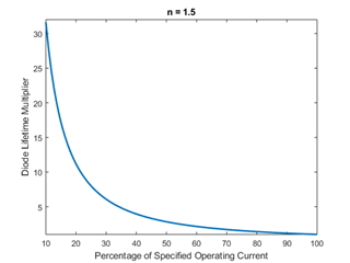
In operation an Integrated circuit's life span is dependent on the circuits design parameters. The lifetime can be reduced from years to milliseconds through poor design choices. Every choice has an effect.. The question is "how much shorter". In 1970, while working at RCA Labs on GaN and GaP LED development I learned that diode lifetime is dependent on current density and temperature management. (as shown below)
I believe that this demonstrates my thought that the current levels thru the ESD diode will not dramatically shorten the lifespan of the PCF8574.
You stated; "I don't have any data that I could give you for how long it would take for the PCF8574 to become damaged if held within abs max ratings. I would have to talk to the design team to understand how long the ESD structures would last under your conditions." I would ask if you could do that.
You asked for the Forum link https://forum.arduino.cc/t/p-type-mosfet-and-pcf8574/1393532 Removal of R1 would disable the function of the MOSFET. There have been solutions suggested. Additional components would increase loading of Vcc which close to it's limits. Thanks again for your time Barry
It is important to remember that this circuit is NOT pulsed. The output of the PCF8574 is expected to be in a high state 90% of the time. My goal is to turn on the mosfet at intervals of every 5-15 minutes for a minimum of 15 minutes. depending on solar conditions, that might occur 3 times a day or not for 3 days.
I submitted the ticket. I am trying to understand from the design team if it is a DC spec for IOK. I am 95% sure it is a DC spec.
This is an interesting case however. I am sure if you were to have two PCF8574 devices side by side, one that has 10 uA IOK, and the other that has the abs. max of 400 uA, you would most likely see the second device fail much faster than the one that is drawing 10 uA.
This is just my assumption. I need to discuss with design on the implications of the spec. Most of the times, the abs. max specs are usually guard banded. Although we say the abs. max input voltage is +6.5V, it usually has a little more margin than what is in the datasheet. This is most likely the same with the IOK spec. We state +/- 400 uA, but it probably has more margin until permanent damage may occur. In most cases we over design, guard-band, to ensure device reliability and that the datasheet is true to what it says.
According to Jim in the Arduino thread, if IOK was a transient spec, we most likely would have stated somewhere in the datasheet those limitations.
From design perspective, I don't think they are going to get an answer any time soon. From recent discussion, I do think that if 12V or any voltage > abs. max voltage is present on the input pin of PCF8574 will create a reliability concern even if it is clamped indefinitely limited by series resistance. Best practice is to keep the input voltage on the Pxx pin within the recommended operating conditions of the datasheet.
Given this schematic, it looks like when PCF8574 is not driving any voltage signal, the voltage at PXX will be ~ 5V since zener D2 will hold the voltage at that level.
I simulated using LTSPICE with a diode that has a Vz = 5.1V, it looks like in simulation that this will work and be within spec of the datasheet for when PCF8574 is driving LOW, or pulled weakly HIGH.
Designs' comments in reference to the clamping current spec limited by series resistance.
"Looking at the spec and the mechanism of this leakage, it should be fine for long term as well. As long as this current is kept below 100uA across temperature, it should not cause any performance issues as the I/O driver (PMOS driver) of push-pull circuit will see majority of the current when IO pin Voltage > VCC and NMOS driver + ESD cell when pin Voltage < 0V and can safely tolerate without any degradation."