This thread has been locked.

If you have a related question, please click the "Ask a related question" button in the top right corner. The newly created question will be automatically linked to this question.

DP83822I: Power Sequence Support Needed

Part Number: DP83822I

Tool/software:

Hi team,

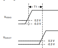
In my customer's ongoing design, 2.5V for VDDIO is generated from 3.3V powering AVD.

So it is impossible to wait for AVD ramp until VDDIO fully ramps up.

So my customer is wondering if it is allowed when VDDIO<AVD+0.3V is kept.

Could you please check it?

If this is not recommended, could you please advise how to address this?

Best regards,

Kazuki Itoh

  • Hi Itoh-san, 

    So my customer is wondering if it is allowed when VDDIO<AVD+0.3V is kept.

    I would say this is not recommended because false detection can occur. The false detection occurs when AVD finishes ramping and samples the VDDIO voltage while this rail is still ramping. In this case, the PHY can incorrectly read the VDDIO voltage before the rail finishes ramping.


    As a workaround, could the customer use 3.3V for VDDIO? If this is not an option, I suggest possibly ramping VDDIO and AVD at the same time if this can be done. 

    Please let me know your thoughts. 

    Best,
    J


  • Hi J,

    Thanks. As the customer is using 2.5V for MAC interface, the VDDIO is set to 2.5V.

    They determined to ramp VDDIO and AVD at the same time.

    Best regards,

    Kazuki Itoh

  • Hi Itoh-san,

    Great to hear! Let me know if the customer has additional questions.

    Best,

    J

  • Hi J,

    I have a couple of questions from the customer.

    1. How the T1: ±100ms is determined? Is that measured by 50% of the each rail?
    2. If yes, it looks like the ramp up at the same time is allowed because it is within ±100ms T1 range.
      Given that, AVD (3.3V) ramps up before VDDIO(2.5V) in my customer's design.
      Is it still okay? Could you please review the waveform below?
    3. Could you let me know the current and power consumption of VDDIO=2.5V and AVD=3.3V respectively?
      It's not found on Table 10-1 with this combination.

    Best regards,

    Kazuki Itoh

  • Hi Itoh-san, 

    1. That is correct. 
    2. The waveform except that there is a initial ramp of 1V for 2.5V is good. Please ensure that the customer can follow both VDDIO<AVD+0.3V and simultaneous ramp up if possible. 
    3. I couldn't find this data on our end.

    Please let me know. 

    Best,

    J

  • Hi J,

    About #2, yes, there's initial 1V ramp, but it's still within T1=±100ms specified in the datasheet. Is it not allowed?

    About #3, my customer is reffering to Table 10-1 Power Supply Characteristics. However, my customer would like to provide the data under  VDDIO=2.5V and AVD=3.3V. Does it make sense?

    Best regards,

    Kazuki Ioth

  • Hi Itoh-san, 

    2. Yes, timing is fine. I am talking about this comment in the datasheet:
    AVD and VDDIO potential must not exceed 0.3 V prior to supply ramp.

    especially when AVD is not ramped at all to prevent false detection. 

    3. I understand you need 2.5V VDDIO and 3.3V AVD. Unfortunately, we couldn't locate the data and it will have to be collected. This will most likely take couple of weeks.

    Please let me know. 

    Best,
    J

  • Hi J,

    Thank you.

    > Unfortunately, we couldn't locate the data and it will have to be collected. This will most likely take couple of weeks.

    My customer is requesting us to collect the data. It is okay even if it takes a couple of weeks.

    Could youp please support?

    Best regards,

    Kazuki Itoh

  • Hi Itoh-san, 

    We can support this. However, please note that US has Fourth of July holiday so US office will be closed. 
    After we come back from the holiday, we expect collecting data will take two weeks since we do not have power consumption set up currently in the lab. 

    I will keep you updated. 

    Best,
    J

  • Hi J,

    Thank you for taking an action on this. I have one more question.

    Should the power sequence strictly be followed even if the DP83822's RESET_N pin is Low by external pull-down and RESET_N goes high after VDDIO and AVD fully ramping up?
    My customer guesses that the IO pins including hard strap doesn't operate unless RESET_N pin goes high so the false detection can be avoided.

    Best regards,

    Kazuki Itoh

  • Hi Itoh-san, 

    We recommend to follow the power sequence even when the RESET_N pin is low since the recommendation was given out considering that the the reset signal will be low. But, the customer's understanding is correct that the strapping doesn't sample until RESET_N goes high. 

    Best,
    J

  • Hi J,

    It still doesn't make sense to me.

    Why do you recommend to follow the power sequence when RESET_N is low while the strapping doesn't sample until RESET_N goes high?

    Could you please make it more clear?

    Best regards,

    Kazuki Itoh

  • Hi Itoh-san, 

    We recommend to follow the power sequence when RESET_N is low to ensure that as the power is brought up the PHY does not initialize and stay in the RESET state so it does not sample strap configurations or VDDIO wrong. 

    Best,
    J

  • Hi Itoh-san, 

    Below is the power measurement result for VDDIO 2.5V and AVD 3.3V. 
    Please let me know if you have any questions about this. 
    DP83822_Power_Measurement.xlsx
    Best,
    J