Part Number: TVS2701
Tool/software:
Hi team,
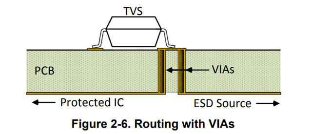
In "12.2 Layout Example" of the datasheet,
the width of the power supply trace seems to be the same length (0.6mm) as the PAD of the IN terminal of the TVS2701.
If the trace width is 0.6mm, the current capacity of the trace is 0.6A.
I want to pass a current of 2.5A or more, so I want to widen the trace width.
If I widen the trace width as in the attached image, will the widened part become a detour path for the current, reducing the ESD protection performance?
How many mm can I widen the trace width without any problems in terms of performance?

Best regards,
Yasuhara