This thread has been locked.

If you have a related question, please click the "Ask a related question" button in the top right corner. The newly created question will be automatically linked to this question.

DS90LV011A: OUTPUT Distortion

Part Number: DS90LV011A
Other Parts Discussed in Thread: DS90LV012A, DS90LV011-12AEVM

Tool/software:

Dear TI team:

We had a project used the DS90LV011A+DS90LV012A for input a 24M HZ CLK. 

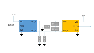
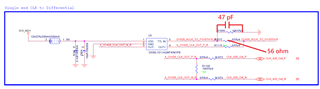
DS90LV011A design as blew. But we found the screen will flick when device on.

Had try add 47pF to GND and series 56 ohm in TTL IN pin.

Issue had been improved but not completely resolved.

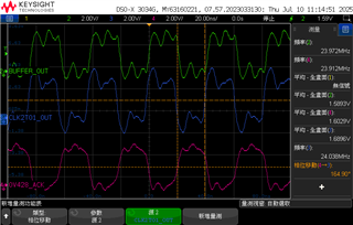
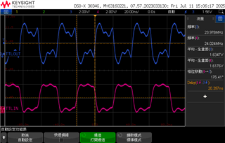
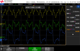
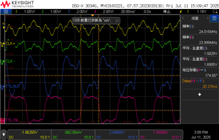
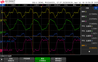
The TTLIN 、 OUT+/-、TTLOUT waveform as blew.

Seem TTLOUT have been attenuated.

Please help these question~

1.How can I fix this problem?

2.Is DS90LV011A can adjust the driving?

3.How far can TTLIN +OUT/- + TTLOUT be in total?


(Use DS90LV011-12AEVM to do experiment. It had same problem.)

Thanks~

Best Regards,

Andy

  • Hi Andy, 

    Sorry you're experiencing this problem. However, there are two things I immediately noticed that could be causing problems: 

    1.) You have a 100 Ohm termination resistor (R1100) on the transmitter side of the LVDS bus. Point-to-point LVDS only requires one termination resistor at the receiver. If you have 2 termination resistors, that will definitely cause issues, but if the only termination resistor on the bus is on the transmitter side, i would still recommend moving it to the receiver. Do you mind sending the schematic of how the DS90LV012A is connected? It would also be very helpful to see the layout since LVDS can be sensitive to how the board is laid out. Can you send that as well?

    2.) You are shorting TTL IN to OUT+ via a 0 Ohm resistor (R1119). However, I see "NA" next to this resistor in green text. Does "NA" mean the same as DNP/DNI where the resistor is not present on the board? Also, can you explain way you added a 56 Ohm resistor and a 47 pF capacitor to these lines? You shouldn't need to attenuate the input clock signal. 

    For your other 2 questions, can you clarify the information you are asking for? DS90LV011A has an internal output current limit of 24 mA, and for max cable length, please refer this app note: How Far, How Fast Can You Operate LVDS Drivers and Receivers? . It looks like a 24 MHz clock (48Mbps) would support ~15m cables with minimal jitter. I'm not sure if this the info you were looking for in your last 2 questions, but if not, please clarify. 

    Regards,

    Matt 

  • Dear Matt,

    Thanks for feedback! Update this problem as below

    Please see ref schematic as attach. (Some part is design by customer so I can't just share the whole schematic.)

    NA mean didn't mount this material only for debug using~

    And sorry for the measure waveform update, previous picture may connect to the wrong GND for TTLOUT.

    The TTLOUT attenuate seem not to be so serious.

    But we still found that TTLIN and TTLOUT had 164.9 degree phase difference.

    I think it's not normal phenomenon. How can I fix this problem?

    Thanks~

    Best Regards,

    Andy

  • Hi Andy, 

    Understood. Assuming the reference schematic you shared is exactly how the design is being implemented, the schematic part of this design should not be causing any issues. Like I mentioned earlier, layout can have a significant effect on the signal integrity as well. If you can't share the layout files, I understand, but please review this app note and make sure you aren't violating any key layout guidelines: High-Speed Layout Guidelines for Reducing EMI for LVDS SerDes Designs

    To make sure the IC itself is not the issue, can you replace the DS90LV011A/12A with fresh units and see if the problem still persists? 

    Also, the waveform labels on your scope captures are not clear to me. Can you show the voltage waveforms for the following pins: TTLIN, OUT+, OUT-, differential voltage between OUT+ and OUT-, and TTLOUT? It looks like the latest scope capture you sent has most of that information where BUFFER_OUT = TTLOUT, OV428_ACK = TTLIN, and CLK2TO1_OUT = the differential voltage between OUT+ and OUT-, however, I'd like to confirm that before making assumptions. Also, please confirm if you are using a proper differential probe to measure the LVDS bus signals and where on the board those signals are being probed from. 

    Regards,

    Matt 

  • Dear Matt,

    We had try many peace of PCB and had the same result. It's seem not to be the single case of IC itself.

    And update waveform as below. 

    Pink Color:TTLIN  (measure close DS90LV011A IC)

    Blue Color:TTLOUT (measure close DS90LV012A IC)

    Yellow Color:CLK+ (measure close DS90LV012A IC)

    Green Color:CLK- (measure close DS90LV012A IC)

    Observed the TTLIN and TTLOUT had a huge degree phase difference.


    Thanks~

    Best Regards,

    Andy

  • Hi Andy,

    If swapping the DS90LV011A/12A out with fresh units does not fix your problem, then your problem lies with how are connecting/laying out your board. Unfortunately, if you cannot share your schematic/layout files, I will not be able to help you anymore since we have confirmed the issue does not lie with our devices. 

    Before I close this out, I will say this is likely due to the LVDS bus impedance not being matched properly. For example, in the original schematic image you shared, you have a trace through R1119 connecting OUT+ to TTLIN. While R1119 is not populated, this trace will still distort the impedance of the bus. I would recommend going through your schematic/layout again and try to remove all unnecessary forms of parasitic capacitance/resistance.

    Please let us know if there's anything else we can do to help. 

    Regards,

    Matt