Part Number: SN65HVD10
Tool/software:
Hi Team,
Can you help to review below sch and layout? Thanks!
There will be 3 solutions applied in one project.
Part Number: SN65HVD10
Tool/software:
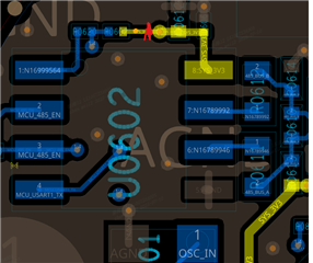
Hi Team,
Can you help to review below sch and layout? Thanks!
There will be 3 solutions applied in one project.