This thread has been locked.

If you have a related question, please click the "Ask a related question" button in the top right corner. The newly created question will be automatically linked to this question.

THVD8000: pulse width distortion

Part Number: THVD8000

Tool/software:

Hi Experts, 

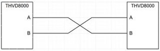
We want to use the THVD8000 in a project. It would simplify the layout if we could cross-connect the differential pins "A" and "B" on the two bus nodes. like this:

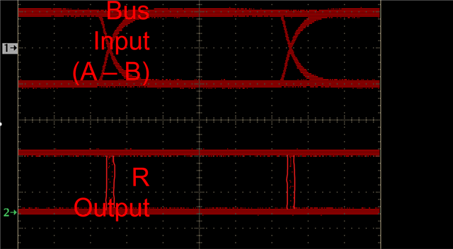
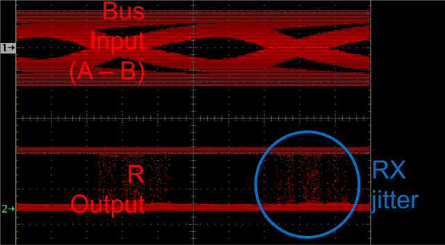
According to the data sheet, the "pulse-width distortion" deteriorates. However, I cannot fully explain what this means. What does this degradation of the "pulse-width distortion" mean?

Can you advise on this, please? 

Regards 

  • Hi Quirin,

    Pulse width distortion degradation - is worded strangely - but the point is that you may see more distortion in the pulse width - i.e. jitter. Basically you can add more jitter to the system by doing this - we don't have a way to determine how much jitter because it is extremely application dependent - but you may not be capped to the +/-2% duty cycle distortion inherent to the part. 

    That being said - I have seen a few instances of designs doing this and they were not having SI issues - there could have been added jitter but it hasn't been enough to compromise those applications. However if you have a really long bus and/or your modulation frequency is higher you will see higher levels of jitter which then could cause issues with the added jitter from the cross wiring. 

    Please let me know if you have any other questions and I will see what I can do. 

    Best,

    Parker Dodson

  • Hello Parker,

    Thank you for your prompt response.

    I originally asked Quirin this question. He was kind enough to forward it to this forum for me.

    Does jitter mean that the two bus signals, 'A' and 'B', are time-shifted with respect to each other? Because this asymmetry would cause EMI distortions, which we are trying to avoid.

    Thank you in advance!

    Florian Regensburger

  • Hi Florian,

    What you describe could be a component adding to the total jitter of the system - but it is more than just that. 

    Jitter is the deviation from ideal periodicity  (usually it is defined as the deviation from true periodicity). Which in a very simplistic example imagine you have a 1kHz square wave with 50% duty cycle - ideally the low and high time would both be 500us - but jitter would impact the pulse width where lets say you have +/-5us of jitter in the system you could see a high time of 495us and low time of 505us (as an example). 

    Here is an example in an RS-485 system (not directly power bus - but explains the behavior pretty clearly with some images):

    First - an image with low output signal jitter - the "R" signal is a bit hard to see so I added rough red outlines to show where the "R" signal transition is occurring. 

    Second image - high jitter 

    These images are long exposure shots of multiple transitions - as you can see in image two the variation of the output RX signal is extremely variable which is going to be bad not only for EMI considerations but also can corrupt data or make accurate data collection very hard. 

    One thing to note is that jitter is going to exist when using this part - there is a +/-2% duty cycle distortion inherent to the part - meaning the modulator has up to a +/-2% jitter inherently. The longer the bus is relative to modulation frequency will also add more jitter to the system. Usually in most RS-485 based systems 5% of jitter is more or less okay (it really will depend on end application) but they can go up to 20% (I generally wouldn't try to go that high - I try to keep it below 10% closer to 5% if possible in a system). 

    We don't have a direct "guide" on length versus distance and jitter on this device (there is a generic RS-485/RS-422 one attached below)

    A couple notes about this graph however:

    1. The x-axis should be divided by 2 and changed to modulation frequency (i.e. instead of 10Mbps on the x-axis it would be 5MHz modulation frequency - and nothing before the 250kbps (which would be 125KHz) is captured.

    2. This assumes you are using 120 ohm twisted pair cabling - which in many Powerbus (THVD80x0) that is not the case - a lot of the time the wiring is not even impedance controlled. 

    We do have a general max length chart that assumes "20%" jitter max for the THVD8000 using more standard power cable:

    If you are under 300m for any of them you probably wouldn't be seeing a ton of jitter - but there is some value in this chart - at least when trying to determine boundary points. 

    As a general rule to reduce jitter in the system:

    1. Use the lowest data rate possible in the system - lets say this is 9.6kbps - then the lowest modulation frequency would be 96KHz - our closest to that on the device is 125KHz - lower modulation frequencies will result in lower jitter for the same bus length. 

    2. This comes at a cost - at 125KHz your coupling inductors will be relatively large - if you only have a couple/few devices on the bus it won't be that big of a deal - but you could still be looking at mH level inductances needed per node. 

    Increasing modulation frequency higher than necessary will shrink inductors but will increase jitter seen on the bus. 

    Please let me know if you have any other questions!

    Best,

    Parker Dodson

  • Hi Parker, 

    thank you for the answer.

    Best regards,

    Florian Regensburger 

  • Hi Florian,

    You are welcome!

    Please don't hesitate to reach out if you have any other questions!

    Best,

    Parker Dodson